1147
Samsung launches the industry's first 28-megapixel BSI CMOS image sensor APS-C format
Good day, Habr!
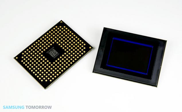
Samsung Electronics has announced a 28-megapixel image sensor APS-C CMOS Digital Camera - S5KVB2. The new sensor has already gone into production - they have supplied a new compact camera Samsung NX1, which was presented last week at the exhibition Photokina 2014 in Cologne, Germany.

The basis of the new development lies in the use of Samsung technology reverse pixel illumination that will improve the sensitivity of each pixel to increase light absorption and peripheral areas by 30%, and consequently - to provide a clear and high-quality images. The metal layers are formed of copper, using the 65-nanometer process technology with low power consumption. This provides a significant advantage over S5KVB2 most common today, image sensors, which are produced by the 180-nanometer process technology using aluminum conductors, namely - a significant reduction in power consumption and heat dissipation. Through the use of the new process technology and the architecture of integrated circuits, the image sensor S5KVB2 also significantly reduces noise during operation.
Since the metal layers are under photodiodes, Samsung engineers got more freedom in the design of their topology, which ultimately will improve sequential read speed. The features of the new sensor S5KVB2 allows not only to obtain high-quality pictures, but UHD-shoot video at 30 frames per second.
Source: habrahabr.ru/company/samsung/blog/237915/
Samsung Electronics has announced a 28-megapixel image sensor APS-C CMOS Digital Camera - S5KVB2. The new sensor has already gone into production - they have supplied a new compact camera Samsung NX1, which was presented last week at the exhibition Photokina 2014 in Cologne, Germany.

The basis of the new development lies in the use of Samsung technology reverse pixel illumination that will improve the sensitivity of each pixel to increase light absorption and peripheral areas by 30%, and consequently - to provide a clear and high-quality images. The metal layers are formed of copper, using the 65-nanometer process technology with low power consumption. This provides a significant advantage over S5KVB2 most common today, image sensors, which are produced by the 180-nanometer process technology using aluminum conductors, namely - a significant reduction in power consumption and heat dissipation. Through the use of the new process technology and the architecture of integrated circuits, the image sensor S5KVB2 also significantly reduces noise during operation.
Since the metal layers are under photodiodes, Samsung engineers got more freedom in the design of their topology, which ultimately will improve sequential read speed. The features of the new sensor S5KVB2 allows not only to obtain high-quality pictures, but UHD-shoot video at 30 frames per second.
Source: habrahabr.ru/company/samsung/blog/237915/
Not sitting: Apple has responded to reports of slanting iPhone 6 and 6 Plus
Agate 9 - Soviet response Apple. Part One


