1558
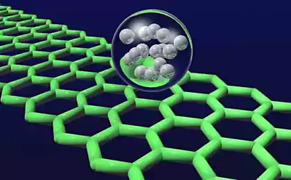
Korean scientists have developed a revolutionary technology to produce graphene
Although graphene consists of widely distributed in nature, carbon, it is very expensive since it has not yet been invented methods of its production on an industrial scale. Relatively simple to get a tiny flakes of graphene. Large single-layer graphene sheet single crystal suitable for use in microelectronics - so far unattainable goal.
Nevertheless, it seems that a breakthrough is imminent. Just a few months ago at the research center named after IBM Thomas J. Watson learned receive 10-centimeter graphene sheets . And on April 3 this year in the journal Science published the results of совместного research scientists from the Institute of Advanced Technology Samsung and Sungkyunkwan University (South Korea), which describes another method to obtain large graphene sheets with perfect structure, potentially suitable for mass production.
The main problem of growing graphene - the presence of areas with different orientation of the crystal lattice, which are formed at the junction of defects. This problem could be avoided if a large sheet of graphene grown from a single crystallization center, but it is very difficult to implement in practice. Korean scientists have found a way to carry out the crystallization of graphene so that all areas in which crystallization began, were oriented in the same and fused into a single unit with no defects. A key element of the new technology - specially treated substrate.
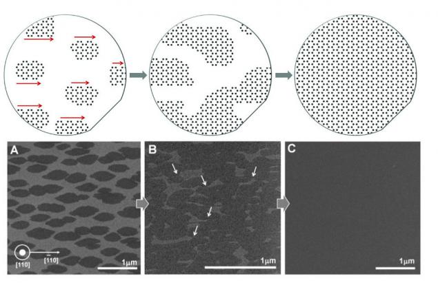
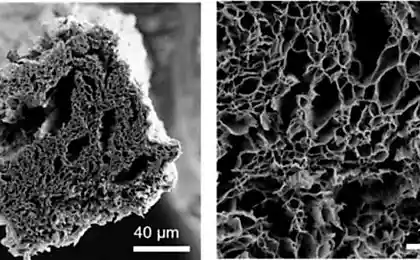
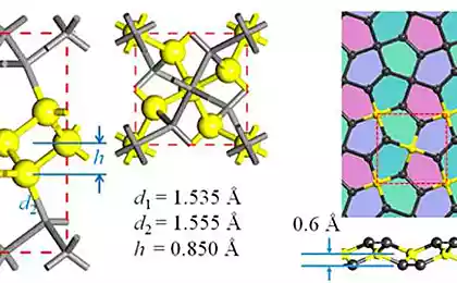
The individual areas of graphene are fused into a single list (at the top - a diagram at the bottom - the image from the microscope) i>
It is based on a common silicon wafer is used for the production of microchips. It is covered with a thin layer of monocrystalline germanium and then its surface is treated with a 10% aqueous solution of hydrogen fluoride (hydrofluoric acid). The acid dissolves the oxide film on the surface of germanium and it forms a layer instead of hydrogen atoms. Such a substrate has two very important properties.
First, the crystal lattice of germanium serves as a template for the settling of carbon atoms - all crystallization centers are oriented the same way, and subsequently fused perfectly. Secondly, it has low adhesion to graphene - it makes it easy to remove creases formed at the junction of different areas of graphene or due to differences in the coefficient of thermal expansion of graphene and Germany. Low adhesion also allows you to easily separate sheet of graphene on a substrate without damaging it. In many other ways to make graphene substrate has to be dissolved. This makes the production disadvantageous since creating a perfectly flat and clean substrate itself is expensive.
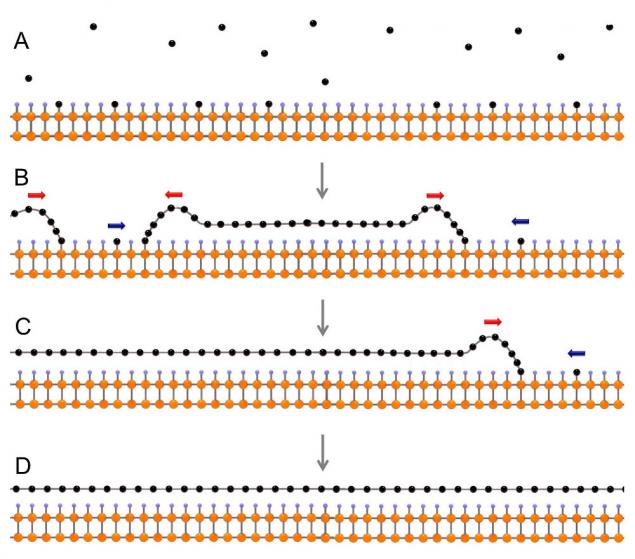
A) Start of carbon deposition; B) the formation of separate areas of graphene; C) region fused into one; D) ready graphene sheet. Marked with black carbon, orange - germany, blue - hydrogen. I>
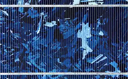
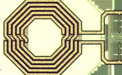
Carbon source is methane. Deposition of carbon on the substrate occurs at a temperature of 900 - 930 degrees Celsius and a pressure of about 13% of atmospheric for a time of from 5 to 120 minutes. Electron microscopy confirmed the absence of defects in the structure and neregulryanostey graphene sheet. Of the as-synthesized graphene researchers succeeded in fabricating a field effect transistor. Laboratory staff Samsung said , which developed technology - "one of the most significant breakthroughs in the history of research on graphene." They believe that this discovery will speed up the industrial development of graphene and open a new era in electronics.
Source: habrahabr.ru/post/218357/
Nevertheless, it seems that a breakthrough is imminent. Just a few months ago at the research center named after IBM Thomas J. Watson learned receive 10-centimeter graphene sheets . And on April 3 this year in the journal Science published the results of совместного research scientists from the Institute of Advanced Technology Samsung and Sungkyunkwan University (South Korea), which describes another method to obtain large graphene sheets with perfect structure, potentially suitable for mass production.
The main problem of growing graphene - the presence of areas with different orientation of the crystal lattice, which are formed at the junction of defects. This problem could be avoided if a large sheet of graphene grown from a single crystallization center, but it is very difficult to implement in practice. Korean scientists have found a way to carry out the crystallization of graphene so that all areas in which crystallization began, were oriented in the same and fused into a single unit with no defects. A key element of the new technology - specially treated substrate.

The individual areas of graphene are fused into a single list (at the top - a diagram at the bottom - the image from the microscope) i>
It is based on a common silicon wafer is used for the production of microchips. It is covered with a thin layer of monocrystalline germanium and then its surface is treated with a 10% aqueous solution of hydrogen fluoride (hydrofluoric acid). The acid dissolves the oxide film on the surface of germanium and it forms a layer instead of hydrogen atoms. Such a substrate has two very important properties.
First, the crystal lattice of germanium serves as a template for the settling of carbon atoms - all crystallization centers are oriented the same way, and subsequently fused perfectly. Secondly, it has low adhesion to graphene - it makes it easy to remove creases formed at the junction of different areas of graphene or due to differences in the coefficient of thermal expansion of graphene and Germany. Low adhesion also allows you to easily separate sheet of graphene on a substrate without damaging it. In many other ways to make graphene substrate has to be dissolved. This makes the production disadvantageous since creating a perfectly flat and clean substrate itself is expensive.

A) Start of carbon deposition; B) the formation of separate areas of graphene; C) region fused into one; D) ready graphene sheet. Marked with black carbon, orange - germany, blue - hydrogen. I>
Carbon source is methane. Deposition of carbon on the substrate occurs at a temperature of 900 - 930 degrees Celsius and a pressure of about 13% of atmospheric for a time of from 5 to 120 minutes. Electron microscopy confirmed the absence of defects in the structure and neregulryanostey graphene sheet. Of the as-synthesized graphene researchers succeeded in fabricating a field effect transistor. Laboratory staff Samsung said , which developed technology - "one of the most significant breakthroughs in the history of research on graphene." They believe that this discovery will speed up the industrial development of graphene and open a new era in electronics.
Source: habrahabr.ru/post/218357/