1430
Samsung made a discovery that can transform the entire consumer electronics industry
Good day, Habr!
Earlier this month, Samsung Electronics has announced the opening of a revolutionary method for producing graphene - a unique material, for which there is the future of electronic devices of the new generation. Development was carried out by specialists of the Institute of advanced technology Samsung (Samsung Advanced Institute of Technology, SAIT) in collaboration with colleagues from Sungkyunkwan University in Seoul.

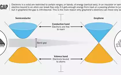
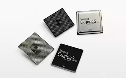
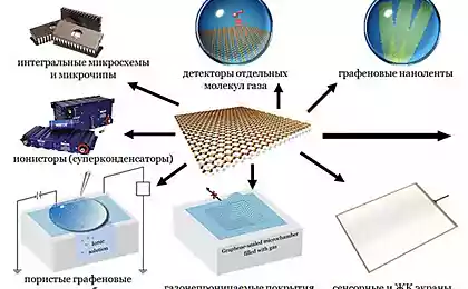
Graphene greatly exceeds used in modern electronics on silicon series semiconductor properties (in particular, a hundred times greater mobility of electrons). He is stronger than steel, has high thermal and electrical conductivity, and finally, very flexible, which suggests its use for the production of flexible displays and wearable devices of the near future.
Samsung Advanced Institute of Technology, in collaboration with the Department of Advanced Materials Science and Engineering Sungkyunkwan University developed a method for the production of single-crystal graphene wafers large area. Leading engineers around the world for a long time to explore ways to produce graphene, but encountered many obstacles. It has been found that the process of multicrystalline synthesis (synthesis of small particles to create a large square plates) worsens the electrical and mechanical characteristics of the material, which limits its application and makes it difficult to process future commercialization.
The new method, developed by SAIT and employees Sungkyunkwan University, allows to synthesize graphene plates in a single crystal, while maintaining electrical and mechanical properties of the material. Efficient technology allows multiple receive monocrystalline graphene on a single semiconductor substrate.
Over the past few decades, the growth of the semiconductor industry was due to the possibility of increasing the area of the produced silicon wafers, while simplifying the process. As the commercial use of graphene is aimed at reducing dependence on silicon industry, it is extremely important to develop a new method for producing a solid crystal graphene large area.
Samsung Electronics Co. Ltd. and Sungkyunkwan University are partners in nanoresearch since 2006. The emergence of new advanced design shows a strong scientific basis of these institutions, which helped them to achieve such outstanding results and become the driving force behind the next generation of technologies.
The study was funded by the Ministry of Education, Science and Technology of Korea, the project program of support of leading researchers (Project to Nurture Leading Creative Researching Experts Program).
Samsung Advanced Institute of Technology was established as an R & D department of Samsung Group in October 1987. The institution is the center of creating advanced technology in accordance with the company's philosophy - the pursuit of new technological developments with a view to change the world for the better. In addition, SAIT is the main technical department of Samsung Group.
Source: habrahabr.ru/company/samsung/blog/219525/
Earlier this month, Samsung Electronics has announced the opening of a revolutionary method for producing graphene - a unique material, for which there is the future of electronic devices of the new generation. Development was carried out by specialists of the Institute of advanced technology Samsung (Samsung Advanced Institute of Technology, SAIT) in collaboration with colleagues from Sungkyunkwan University in Seoul.

Graphene greatly exceeds used in modern electronics on silicon series semiconductor properties (in particular, a hundred times greater mobility of electrons). He is stronger than steel, has high thermal and electrical conductivity, and finally, very flexible, which suggests its use for the production of flexible displays and wearable devices of the near future.
Samsung Advanced Institute of Technology, in collaboration with the Department of Advanced Materials Science and Engineering Sungkyunkwan University developed a method for the production of single-crystal graphene wafers large area. Leading engineers around the world for a long time to explore ways to produce graphene, but encountered many obstacles. It has been found that the process of multicrystalline synthesis (synthesis of small particles to create a large square plates) worsens the electrical and mechanical characteristics of the material, which limits its application and makes it difficult to process future commercialization.
The new method, developed by SAIT and employees Sungkyunkwan University, allows to synthesize graphene plates in a single crystal, while maintaining electrical and mechanical properties of the material. Efficient technology allows multiple receive monocrystalline graphene on a single semiconductor substrate.

Over the past few decades, the growth of the semiconductor industry was due to the possibility of increasing the area of the produced silicon wafers, while simplifying the process. As the commercial use of graphene is aimed at reducing dependence on silicon industry, it is extremely important to develop a new method for producing a solid crystal graphene large area.
Samsung Electronics Co. Ltd. and Sungkyunkwan University are partners in nanoresearch since 2006. The emergence of new advanced design shows a strong scientific basis of these institutions, which helped them to achieve such outstanding results and become the driving force behind the next generation of technologies.
The study was funded by the Ministry of Education, Science and Technology of Korea, the project program of support of leading researchers (Project to Nurture Leading Creative Researching Experts Program).
Samsung Advanced Institute of Technology was established as an R & D department of Samsung Group in October 1987. The institution is the center of creating advanced technology in accordance with the company's philosophy - the pursuit of new technological developments with a view to change the world for the better. In addition, SAIT is the main technical department of Samsung Group.
Source: habrahabr.ru/company/samsung/blog/219525/


Smart City: Are you ready to sacrifice privacy for the sake of efficiency?
Fingerprint scanner in Samsung Galaxy S5 is also vulnerable