2468
As graphene, only phosphorus
Scientists are actively exploring the possibility of obtaining new materials similar to graphene - consisting of a layer of material one atom thick. Significant progress has recently been demonstrated in obtaining phosphorus - material consisting of a single layer of phosphorus atoms.

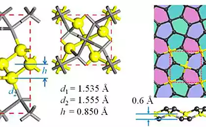
The crystal structure of phosphorus (Credit: Han Liu et al. )
In January of this year were published work of two independent groups, American and kitayskoy , who managed to make significant progress in the preparation of phosphorus. Get phosphorus from the so-called black phosphorus - layered material similar to graphite, from which the graph. Black phosphorus has been known since the 1960s, but only in 2013, attempts were made to distinguish it from a separate layer. In the works in question, black phosphorus was cleaned to a thickness of two - three atomic layers. It is interesting that, as in the first receipt of graphene in 2004, to remove unnecessary layers of adhesive tape used banal.
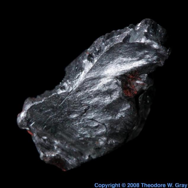
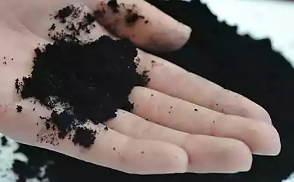
Appearance of black phosphorus (Credit: Theodore W. Gray)
Getting new materials consisting of a single layer of atoms of various substances become in recent years one of the most notable trends in materials science. Scientists have even dubbed this trend "postgrafenovoy era».
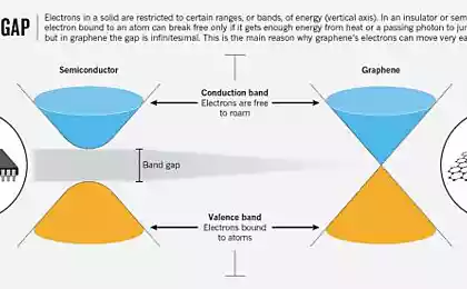
Graphene is a single layer of carbon atoms, has unique properties which make it virtually ideal for use in electronic devices. In particular, graphene is exceptionally high electron mobility, that is a good conductor of electricity and heat. The problem is that graphene is not the so-called band gap - an energy range, which have electron-smoking. The presence of such a zone is highly desirable, since it is the basis of all modern semiconductor electronics, allowing the creation of important elements such as diodes and transistors.
It is therefore actively being sought substances with high electron mobility, and at the same time with the presence of the forbidden zone. Since the high conductivity of graphene is largely due to its two-dimensional, flat structure, and then looking for new materials include those substances that are capable of forming a two-dimensional grid. In July 2013 by the numerical simulation managed to find 92 candidate in such materials, but their experimental receipt became associated with many difficulties.
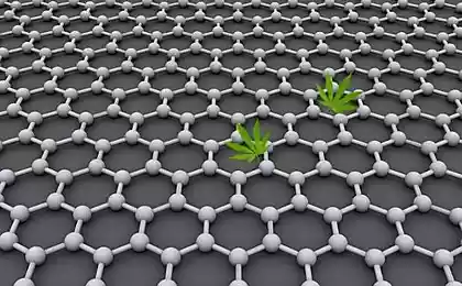
As graphene phosphorus hexagons includes, but is not completely flat - some atoms are slightly above the plane, the other - below. It is, however, slightly slows down the electrons compared to graphene. At the same time, the phosphorus has a band gap, allowing it to different conditions that conduct electricity, it is not.
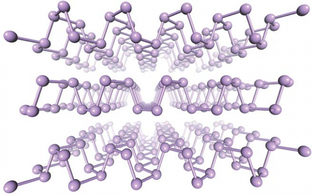
Another illustration of the crystal structure of phosphorus (Credit: Likai Li et al. )
Despite the fact that to achieve the thickness of a single layer, ie, to obtain pure phosphorus, has not yet succeeded, scientists are optimistic. For example, it was shown that even in samples obtained comparable velocity electrons with another candidate "postgrafeny" - molybdenum disulphide consisting of molybdenum and sulfur atoms. The presence of phosphorus atoms in the structure of only one substance - phosphorus - not two, makes the new material is more attractive in terms of ease of manufacture.
Phosphorus is not only an analogue of a graph consisting of one type of atom. Previously managed to get a monatomic layers of silicon - silicon - and Germany - Germany. Both of these materials have higher electric conductivity than the phosphor, but also as graphene do not have a band gap. Theoretically, the more interesting candidate is Stan - monatomic layer of tin, and has a high electron mobility and band gap, but predicted only in 2013 and so far no one has received.
A common problem of all the content at issue is their instability. In the air, they are beginning to oxidize and break down quickly. Special tricks, which managed to stabilize the silicon in 2012, still does not allow the use of this material in actual devices. Phosphorus should be more stable than its competitors, but its production is more complicated: for black phosphorus modification of high purity is required to put under huge pressure. The process of further removal of layers is also not yet optimized.
In any case, the very possibility of a two-dimensional material with a band gap is attractive enough to continue research in this area, and the potential commercial success promises to cover any temporary costs.
In preparing the text used материалы Nature News .
Source: habrahabr.ru/post/212045/

The crystal structure of phosphorus (Credit: Han Liu et al. )
In January of this year were published work of two independent groups, American and kitayskoy , who managed to make significant progress in the preparation of phosphorus. Get phosphorus from the so-called black phosphorus - layered material similar to graphite, from which the graph. Black phosphorus has been known since the 1960s, but only in 2013, attempts were made to distinguish it from a separate layer. In the works in question, black phosphorus was cleaned to a thickness of two - three atomic layers. It is interesting that, as in the first receipt of graphene in 2004, to remove unnecessary layers of adhesive tape used banal.

Appearance of black phosphorus (Credit: Theodore W. Gray)
Getting new materials consisting of a single layer of atoms of various substances become in recent years one of the most notable trends in materials science. Scientists have even dubbed this trend "postgrafenovoy era».
Graphene is a single layer of carbon atoms, has unique properties which make it virtually ideal for use in electronic devices. In particular, graphene is exceptionally high electron mobility, that is a good conductor of electricity and heat. The problem is that graphene is not the so-called band gap - an energy range, which have electron-smoking. The presence of such a zone is highly desirable, since it is the basis of all modern semiconductor electronics, allowing the creation of important elements such as diodes and transistors.
It is therefore actively being sought substances with high electron mobility, and at the same time with the presence of the forbidden zone. Since the high conductivity of graphene is largely due to its two-dimensional, flat structure, and then looking for new materials include those substances that are capable of forming a two-dimensional grid. In July 2013 by the numerical simulation managed to find 92 candidate in such materials, but their experimental receipt became associated with many difficulties.
As graphene phosphorus hexagons includes, but is not completely flat - some atoms are slightly above the plane, the other - below. It is, however, slightly slows down the electrons compared to graphene. At the same time, the phosphorus has a band gap, allowing it to different conditions that conduct electricity, it is not.

Another illustration of the crystal structure of phosphorus (Credit: Likai Li et al. )
Despite the fact that to achieve the thickness of a single layer, ie, to obtain pure phosphorus, has not yet succeeded, scientists are optimistic. For example, it was shown that even in samples obtained comparable velocity electrons with another candidate "postgrafeny" - molybdenum disulphide consisting of molybdenum and sulfur atoms. The presence of phosphorus atoms in the structure of only one substance - phosphorus - not two, makes the new material is more attractive in terms of ease of manufacture.
Phosphorus is not only an analogue of a graph consisting of one type of atom. Previously managed to get a monatomic layers of silicon - silicon - and Germany - Germany. Both of these materials have higher electric conductivity than the phosphor, but also as graphene do not have a band gap. Theoretically, the more interesting candidate is Stan - monatomic layer of tin, and has a high electron mobility and band gap, but predicted only in 2013 and so far no one has received.
A common problem of all the content at issue is their instability. In the air, they are beginning to oxidize and break down quickly. Special tricks, which managed to stabilize the silicon in 2012, still does not allow the use of this material in actual devices. Phosphorus should be more stable than its competitors, but its production is more complicated: for black phosphorus modification of high purity is required to put under huge pressure. The process of further removal of layers is also not yet optimized.
In any case, the very possibility of a two-dimensional material with a band gap is attractive enough to continue research in this area, and the potential commercial success promises to cover any temporary costs.
In preparing the text used материалы Nature News .
Source: habrahabr.ru/post/212045/
Unfulfilled expectations: what is planned and what happened in the "Space Shuttle"
News and trends in wearable gadgets
