822
Nanomaterials: on the verge of science fiction.
That distant time when our ancestors were smart enough to use the simple production of food items, has become a big explosion in the development of technologies. At first, people used "ready" instruments like sticks and stones. Then they learned how to turn them into something more suitable for use. Then he learned how to smelt bronze, and a little later, it became clear that she is not perfect. They began to use iron ... Since then, mankind has opened up countless different materials with a wide variety of properties. Today Materials reborn: scientists are developing their own materials in accordance with the desired characteristics.

Nanotechnology
Probably all at least once a week to hear the word. In the general public, it has long been associated with something in between advanced science, magic and charlatanism, and scientists continue to add magical prefix "nano" in order to obtain substantial grant. Let's understand what nanotechnologies are and what they can offer us in the near and distant future.
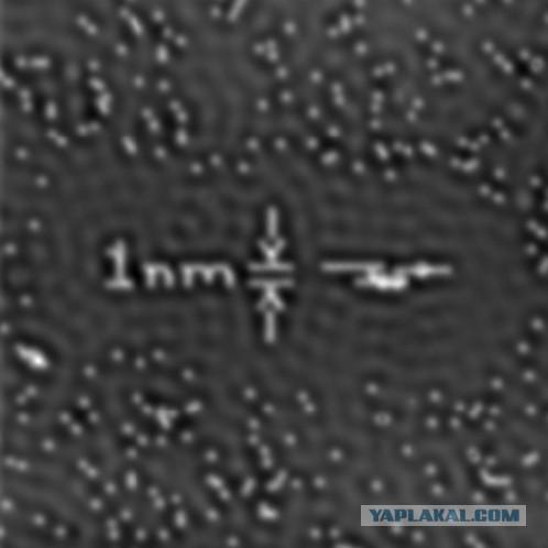
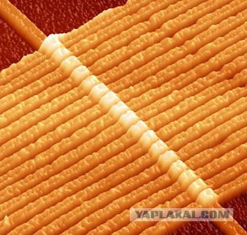
First of all, a nanometer (nm) - is one billionth of a meter. Several facts to sense scale: bristles growing at a rate of 5 nm per second, the diameter of the DNA double helix is around 2 nm, and the thickness of a human hair - between 20 and 150 000 nm depending on the color. At the same time the diameter of the helium atom, - 0, 1 nm. Therefore, nanotechnology is meant by the creation and manipulation of polyhydric structures whose dimensions in at least one dimension (length, width or thickness) are less than 100 nm.
The fact that the properties of matter consisting of such particles are significantly different from the same material in a more familiar to us (compact) form. As we approach the atomic scale is greatly increased surface area materials (total surface area divided by mass). Strong role of quantum-mechanical effects. Often they determine new surprising and often unexpected properties of nanostructured materials.
For example: in nanoscale significantly increases the ability of agents to enter into chemical reactions. In everyday life, aluminum - inert metal in foil from which you can easily bake meat in the oven. But the aluminum nanoparticles are added as catalyst to the solid rocket fuel, which greatly increases the heat output and efficiency.
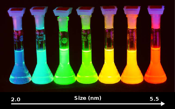
Also significantly change the optical properties of substances. For example, unremarkable in the macrocosm semiconductor - cadmium selenide - at the nanoscale fluorescence colors of the rainbow, the color depends only on the particle diameter. This property of fluorescent nanoparticles (so called quantum dots) have long been used in lasers and biology, but also has a good chance to find application in the manufacture of color displays and flexible in medical diagnosis.
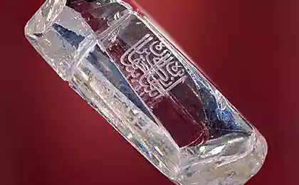
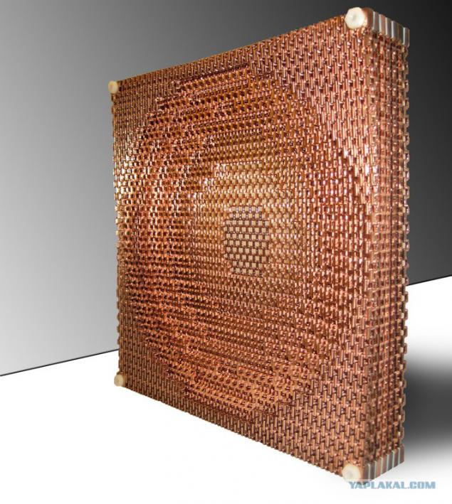
You should not assume that nanotechnology - is something artificial, invented by man. In fact, many ideas borrowed from nature. For example, recently, scientists from the California Institute of Technology, led by Professor Greer constructed heavy-duty material, which consists of "nanobalok" titanium nitride. How do you need to connect the structural elements, the researchers assembled in marine sponges. The resulting nanolattices 85% consists of air, but many times the strength of the source material. And with it you will surely met: it has long been used as a heat resistant coating for steel parts as well as ... for the manufacture of dentures and color domes of Orthodox churches, as in everyday life is like gold.
Lotus leaves and many other tropical plants hardly retain water on its surface. Nanomaterials that mimic the structure of the leaf surface, now sold as a superhydrophobic (water-repellent) and superoleofobnogo (oil-repellent) coating.
Knowing the initial principle, it is possible to develop a coating with a completely opposite properties - superhydrophilic. Such materials can be used for manufacturing a membrane filter for deep water purification. In our bodies play their role proteins aquaporins in large numbers contained in the renal tubules.
The production of nanomaterials
Naturally, no matter how wonderful properties of nanomaterials may be the main criterion of their mass implementation is low cost production. Typically, laboratory scientists have to deal with small samples. Thus, the above-described nanostructured titanium nitride was obtained in the form of a cube with edge of 1 mm. That's enough to measure its performance, but you will agree - to talk about industrial production is still too early.
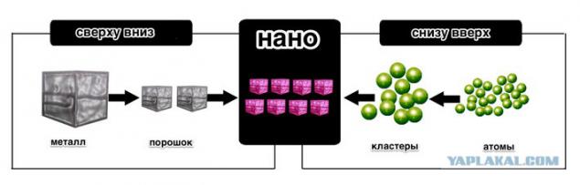
Currently, scientists use two main approaches for the preparation of nanostructured materials: the development of "bottom-up" and "top down". As you might guess, the first involves the assembly of nanomaterials from individual atoms, and the second, on the contrary, based on the fragmentation of larger aggregates.
Both approaches have their drawbacks. If in the case of the development of "bottom-up" the main problem is the organization of disordered particles obtained, the approach of "top-down" provides high accuracy, but very labor-intensive. Therefore, at present a large number of scientific attention is directed to the study of controlled self-organization of nanoparticles. Particularly high expectations associated with the development of the principles of non-equilibrium self-organization. But it is nothing like the principle of the living organisms. It must be admitted that in the creation of nanostructures and nanomachines nature is still far ahead of us.
Here are some of the latest achievements of nanomaterials that may, in a few years our world will change beyond recognition.
Graphene
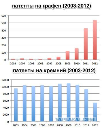
This substance, for the discovery of which was given the Nobel Prize for physics in 2010, is truly a champion in the number of published scientific articles about it. And deservedly: range of unique properties and applications of graphene is amazing. This is despite the fact that you can get the material with just a piece of graphite and stationery scotch! Some optimists now believe that the XXI century will be the century of graphene. What's so special about it?
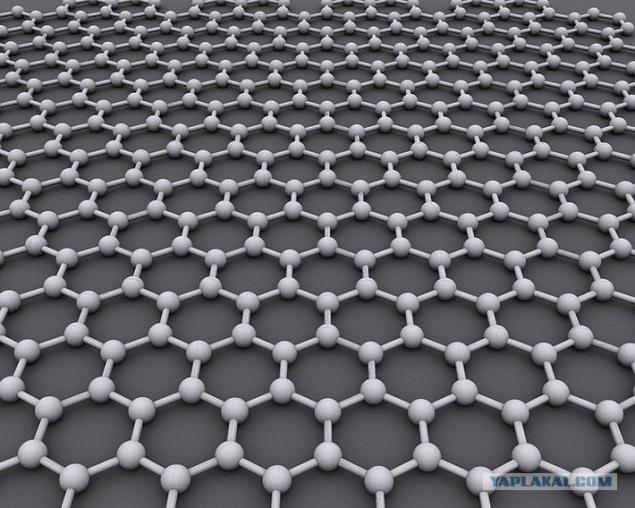
First of all, unlike all the things that surround us, graphene - dimensional material. Essentially this plane, consisting of carbon atoms forming the hexagons in bee cells. Therefore, the graph has a very high specific surface area - it is itself only the surface.
Like its progenitor of a three-dimensional (graphite), graphite - a good conductor. In this two-dimensional due to its resistivity at room temperature is lower than that of silver, and the thermal conductivity is 10 times higher than copper. Needless to say, the transistors based on graphene is much faster than silicon? And all this despite the fact that the material is transparent and flexible.
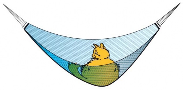
Graphene also has a unique mechanical properties: it is firmer and stronger than a diamond, but can be extended over a quarter of its length. Thus, according to Nobel Prize winners in 2010, graphene hammock area in square meter able to withstand the weight of 4-pound cat, and while he would weigh less than a milligram - like cat's whisker.
The appendage all the unique properties of graphene can be also controlled, for example by using a magnetic field of different substrates or by creating composite materials. And if you do it nanometer holes, the graphene can be made effective filters for desalination!
Unlike many other nanomaterials mass production of graphene is relatively cheap and has actively developed by leading electronics manufacturers.
Topological insulators
This material is an insulator inside, but with the atoms on the surface, in which electrons can be close to the conduction band. Therefore, the motion of electrons in a topological insulators can only be on the surface. As a consequence, there is resistance to a minimum, and the electron can easily accelerate to near the speed of light without backscattering and warming of the conductive layer.
The theoretical possibility of their existence was predicted in 2007, and soon were derived materials with desired properties of bismuth telluride and selenide.
Due to its properties of topological insulators may in the near future become a replacement for semiconductors. An additional advantage over their semiconductors is low sensitivity to impurities. Moreover, in fact they are both conductors and insulators own.
Another notable feature of these materials is that the spin (magnetic moment) of the electrons in the surface layer of a quantum-mechanically connected to its pulse. Until now, at the atomic level of physics could manipulate only electrical (not magnetic) fields. The creation of topological insulators allows us to hope that soon this technological gap will be eliminated and will open the way to an entirely new class of devices based on "spintronics" (by analogy with electronics). And this is a direct path to the creation of quantum computers that can perform calculations for which modern supercomputers would take an astronomical amount of time.
Memristors
More than 40 years ago, the Chinese physicist Leon Chua theoretically predicted the existence of the "missing" fourth basic element of the electrical circuit connecting the electric charge and magnetic flux. In addition to the well-known resistors (connecting voltage and current), capacitors (voltage and charge) and an inductance (current and magnetic flux), he described the properties of hypothetical element - the memristor.
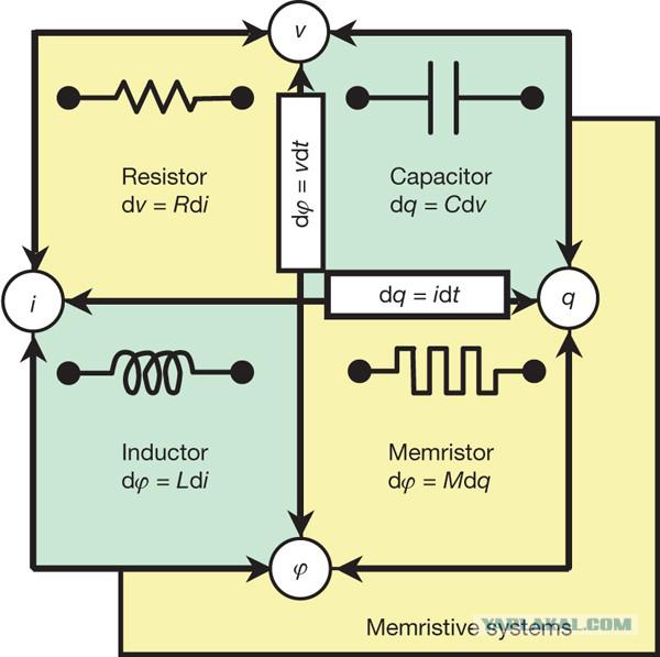
In 2008, a group of scientists from Hewlett-Packard reported in the journal Nature on the first real device of this type. It consisted of nanofilms (50 nm) of titanium oxide sandwiched between titanium and platinum electrodes (each 5 nm thick). A unique feature of the device is its ability to change its own resistance and therefore store information, and the size (2010 HP engineers have brought them to the 3 × 3 nm) and speed (1 GHz) make clear their huge potential.
By the end of 2013 the company plans to start serial production of the first memory devices based on memristor, which will soon be replaced are called "bulky» flash, SSD and so on. D.
As for the scientific value of the memristor, their discovery has the potential to make a revolution in neuroscience. The fact that the collected sufficiently simple circuit devices behave like human neurons. Early experiments have shown that such circuits are capable of "remembering" and "forgetting" information, the learning is performed on the same principle on which the working cells in our brain. The value of this property for the development of artificial intelligence is evident.
Metamaterials
To create something new - in human nature. If something does not exist by itself, then why not do it. Metamaterials - it's completely artificial devices, has properties that are in nature simply does not. They consist of ordered nanoelements such as nanoelectronic circuits. Strict organization enhances the properties of the individual components and enables metamaterials to show them in the macrocosm.
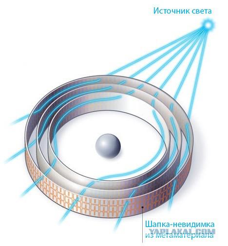
As a result metamaterials exhibit some unique electromagnetic, optical, acoustic, mechanical and other properties. Thus, the first 10-micrometer-dimensional "cap of invisibility" was created precisely using metamaterial-based nanokolets gold and PMMA (plexiglass). Nanoelements "cap" arranged so that the light incident on its surface that surrounds the contour of the material and exits from the opposite side without distortion. Therefore, the observer and the "cap" and the subject of it invisible. A similar principle can be applied to protect the buildings against earthquakes - by trace seismic waves around the object under protection.
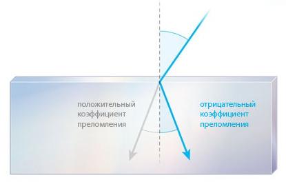
Other applications of metamaterials - the so-called superlens. They consist of a synthetic material having a negative refractive index. Superlens allow focus light on a site smaller than the wavelength, thus opening up new horizons in optical microscopy: they will directly observe the biological macromolecules (DNA and proteins), and create an even more tiny computer chips. Acoustic superlens analogues in the future improve the quality of ultrasound diagnosis.
List the achievements of nanotechnology can be long, as well as a dream on our nanobuduschego. But we must clearly understand what nanotechnology is - it's not magic and not a panacea. The technological revolution - is a continuous process, from the Stone Age to the present day. It is happening here and now, going on hands Curious people and for the people.
Source: Vyacheslav Bernat. Photo: Berkeley Laboratory, California Institute of Technology, IBM, Intech Open Science, Inverstor Intel, Massachusetts Institute of Technology, Nature, Nobel Committee, Wikipedia
Source:

Nanotechnology
Probably all at least once a week to hear the word. In the general public, it has long been associated with something in between advanced science, magic and charlatanism, and scientists continue to add magical prefix "nano" in order to obtain substantial grant. Let's understand what nanotechnologies are and what they can offer us in the near and distant future.

First of all, a nanometer (nm) - is one billionth of a meter. Several facts to sense scale: bristles growing at a rate of 5 nm per second, the diameter of the DNA double helix is around 2 nm, and the thickness of a human hair - between 20 and 150 000 nm depending on the color. At the same time the diameter of the helium atom, - 0, 1 nm. Therefore, nanotechnology is meant by the creation and manipulation of polyhydric structures whose dimensions in at least one dimension (length, width or thickness) are less than 100 nm.
The fact that the properties of matter consisting of such particles are significantly different from the same material in a more familiar to us (compact) form. As we approach the atomic scale is greatly increased surface area materials (total surface area divided by mass). Strong role of quantum-mechanical effects. Often they determine new surprising and often unexpected properties of nanostructured materials.
For example: in nanoscale significantly increases the ability of agents to enter into chemical reactions. In everyday life, aluminum - inert metal in foil from which you can easily bake meat in the oven. But the aluminum nanoparticles are added as catalyst to the solid rocket fuel, which greatly increases the heat output and efficiency.
Also significantly change the optical properties of substances. For example, unremarkable in the macrocosm semiconductor - cadmium selenide - at the nanoscale fluorescence colors of the rainbow, the color depends only on the particle diameter. This property of fluorescent nanoparticles (so called quantum dots) have long been used in lasers and biology, but also has a good chance to find application in the manufacture of color displays and flexible in medical diagnosis.

You should not assume that nanotechnology - is something artificial, invented by man. In fact, many ideas borrowed from nature. For example, recently, scientists from the California Institute of Technology, led by Professor Greer constructed heavy-duty material, which consists of "nanobalok" titanium nitride. How do you need to connect the structural elements, the researchers assembled in marine sponges. The resulting nanolattices 85% consists of air, but many times the strength of the source material. And with it you will surely met: it has long been used as a heat resistant coating for steel parts as well as ... for the manufacture of dentures and color domes of Orthodox churches, as in everyday life is like gold.
Lotus leaves and many other tropical plants hardly retain water on its surface. Nanomaterials that mimic the structure of the leaf surface, now sold as a superhydrophobic (water-repellent) and superoleofobnogo (oil-repellent) coating.
Knowing the initial principle, it is possible to develop a coating with a completely opposite properties - superhydrophilic. Such materials can be used for manufacturing a membrane filter for deep water purification. In our bodies play their role proteins aquaporins in large numbers contained in the renal tubules.
The production of nanomaterials
Naturally, no matter how wonderful properties of nanomaterials may be the main criterion of their mass implementation is low cost production. Typically, laboratory scientists have to deal with small samples. Thus, the above-described nanostructured titanium nitride was obtained in the form of a cube with edge of 1 mm. That's enough to measure its performance, but you will agree - to talk about industrial production is still too early.
Currently, scientists use two main approaches for the preparation of nanostructured materials: the development of "bottom-up" and "top down". As you might guess, the first involves the assembly of nanomaterials from individual atoms, and the second, on the contrary, based on the fragmentation of larger aggregates.
Both approaches have their drawbacks. If in the case of the development of "bottom-up" the main problem is the organization of disordered particles obtained, the approach of "top-down" provides high accuracy, but very labor-intensive. Therefore, at present a large number of scientific attention is directed to the study of controlled self-organization of nanoparticles. Particularly high expectations associated with the development of the principles of non-equilibrium self-organization. But it is nothing like the principle of the living organisms. It must be admitted that in the creation of nanostructures and nanomachines nature is still far ahead of us.
Here are some of the latest achievements of nanomaterials that may, in a few years our world will change beyond recognition.

Graphene
This substance, for the discovery of which was given the Nobel Prize for physics in 2010, is truly a champion in the number of published scientific articles about it. And deservedly: range of unique properties and applications of graphene is amazing. This is despite the fact that you can get the material with just a piece of graphite and stationery scotch! Some optimists now believe that the XXI century will be the century of graphene. What's so special about it?

First of all, unlike all the things that surround us, graphene - dimensional material. Essentially this plane, consisting of carbon atoms forming the hexagons in bee cells. Therefore, the graph has a very high specific surface area - it is itself only the surface.

Like its progenitor of a three-dimensional (graphite), graphite - a good conductor. In this two-dimensional due to its resistivity at room temperature is lower than that of silver, and the thermal conductivity is 10 times higher than copper. Needless to say, the transistors based on graphene is much faster than silicon? And all this despite the fact that the material is transparent and flexible.
Graphene also has a unique mechanical properties: it is firmer and stronger than a diamond, but can be extended over a quarter of its length. Thus, according to Nobel Prize winners in 2010, graphene hammock area in square meter able to withstand the weight of 4-pound cat, and while he would weigh less than a milligram - like cat's whisker.

The appendage all the unique properties of graphene can be also controlled, for example by using a magnetic field of different substrates or by creating composite materials. And if you do it nanometer holes, the graphene can be made effective filters for desalination!
Unlike many other nanomaterials mass production of graphene is relatively cheap and has actively developed by leading electronics manufacturers.

Topological insulators
This material is an insulator inside, but with the atoms on the surface, in which electrons can be close to the conduction band. Therefore, the motion of electrons in a topological insulators can only be on the surface. As a consequence, there is resistance to a minimum, and the electron can easily accelerate to near the speed of light without backscattering and warming of the conductive layer.
The theoretical possibility of their existence was predicted in 2007, and soon were derived materials with desired properties of bismuth telluride and selenide.
Due to its properties of topological insulators may in the near future become a replacement for semiconductors. An additional advantage over their semiconductors is low sensitivity to impurities. Moreover, in fact they are both conductors and insulators own.
Another notable feature of these materials is that the spin (magnetic moment) of the electrons in the surface layer of a quantum-mechanically connected to its pulse. Until now, at the atomic level of physics could manipulate only electrical (not magnetic) fields. The creation of topological insulators allows us to hope that soon this technological gap will be eliminated and will open the way to an entirely new class of devices based on "spintronics" (by analogy with electronics). And this is a direct path to the creation of quantum computers that can perform calculations for which modern supercomputers would take an astronomical amount of time.

Memristors
More than 40 years ago, the Chinese physicist Leon Chua theoretically predicted the existence of the "missing" fourth basic element of the electrical circuit connecting the electric charge and magnetic flux. In addition to the well-known resistors (connecting voltage and current), capacitors (voltage and charge) and an inductance (current and magnetic flux), he described the properties of hypothetical element - the memristor.

In 2008, a group of scientists from Hewlett-Packard reported in the journal Nature on the first real device of this type. It consisted of nanofilms (50 nm) of titanium oxide sandwiched between titanium and platinum electrodes (each 5 nm thick). A unique feature of the device is its ability to change its own resistance and therefore store information, and the size (2010 HP engineers have brought them to the 3 × 3 nm) and speed (1 GHz) make clear their huge potential.
By the end of 2013 the company plans to start serial production of the first memory devices based on memristor, which will soon be replaced are called "bulky» flash, SSD and so on. D.
As for the scientific value of the memristor, their discovery has the potential to make a revolution in neuroscience. The fact that the collected sufficiently simple circuit devices behave like human neurons. Early experiments have shown that such circuits are capable of "remembering" and "forgetting" information, the learning is performed on the same principle on which the working cells in our brain. The value of this property for the development of artificial intelligence is evident.

Metamaterials
To create something new - in human nature. If something does not exist by itself, then why not do it. Metamaterials - it's completely artificial devices, has properties that are in nature simply does not. They consist of ordered nanoelements such as nanoelectronic circuits. Strict organization enhances the properties of the individual components and enables metamaterials to show them in the macrocosm.

As a result metamaterials exhibit some unique electromagnetic, optical, acoustic, mechanical and other properties. Thus, the first 10-micrometer-dimensional "cap of invisibility" was created precisely using metamaterial-based nanokolets gold and PMMA (plexiglass). Nanoelements "cap" arranged so that the light incident on its surface that surrounds the contour of the material and exits from the opposite side without distortion. Therefore, the observer and the "cap" and the subject of it invisible. A similar principle can be applied to protect the buildings against earthquakes - by trace seismic waves around the object under protection.

Other applications of metamaterials - the so-called superlens. They consist of a synthetic material having a negative refractive index. Superlens allow focus light on a site smaller than the wavelength, thus opening up new horizons in optical microscopy: they will directly observe the biological macromolecules (DNA and proteins), and create an even more tiny computer chips. Acoustic superlens analogues in the future improve the quality of ultrasound diagnosis.

List the achievements of nanotechnology can be long, as well as a dream on our nanobuduschego. But we must clearly understand what nanotechnology is - it's not magic and not a panacea. The technological revolution - is a continuous process, from the Stone Age to the present day. It is happening here and now, going on hands Curious people and for the people.
Source: Vyacheslav Bernat. Photo: Berkeley Laboratory, California Institute of Technology, IBM, Intech Open Science, Inverstor Intel, Massachusetts Institute of Technology, Nature, Nobel Committee, Wikipedia
Source: