2467
This is Science: News from graphene fields
The discovery of graphene - a one-dimensional semiconductor - and a description of its properties in 2004 brought its creators Geim and Novoselov the Nobel Prize in the year 2010 but has decades after the discovery of their followers intensively implemented in life and offer a variety of applications such unique material from lubrication to vacuum transistors . < br />
At the beginning of this year was published article "Graphene - life or death?» , In which we analyzed in perspective and partly consequences widespread implementation of graphene as the basis of future microelectronics. Well, let's see what today we can offer scientists a framework for the introduction of graphene replacement to traditional materials.
Summary of graphene h4> Graphene - dimensional material consisting of sp 2 sup > -gibridizovannyh carbon atoms which has a number of interesting from the point of view of physics properties.
The most important and unique of them - the electrical characteristics. Graphene is the one hand, has virtually zero запрещённую area and very light, electrons and holes, which makes it a perfect conductor, able to conduct signals faster than any other material on the planet. However sp 2 sup> hybridization of carbon atoms also allows for a modification to give, for example, an insulator or a semiconductor. Plus, the change between the conducting and semiconducting states depends on the width of the graphene ribbons .
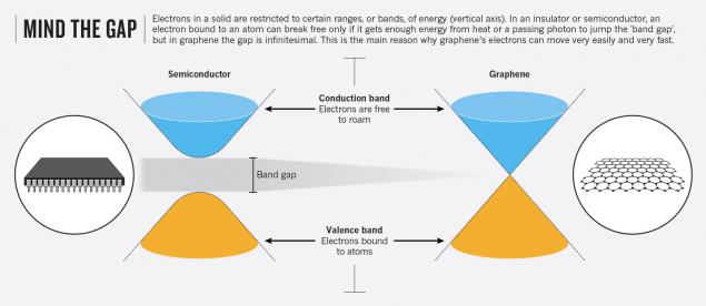
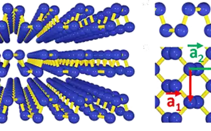
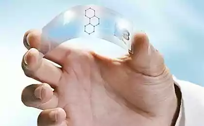
On the other hand it is flexible, i.e. bends, thus demonstrating the unique and unattainable tensile strength - to about 1000 GPa, which is about 100 times higher than that of steel. A collapsed into a tube graphene - a carbon nanotube, which can also be used in electronic devices; its diameter may range from 1.5 nm to several hundred nm.
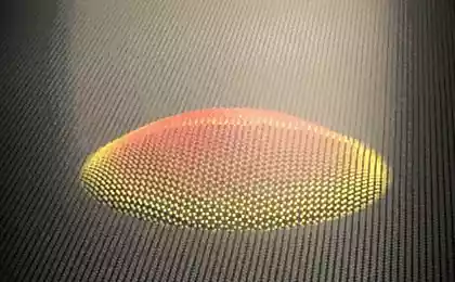
And finally, he, graphene is transparent, that is just perfect as a replacement for the road - mainly due to India - ITO acronym> in modern displays and partly LEDs. However, two-dimensional systems themselves are not stable. Thus, the problem of creating a perfectly smooth graphene coating on any surface - Heavy scientific and engineering problems.
Perhaps with the last property and begin.

LED or LED graphene-based h4>
remarochka. I> If we look at the LED itself (in a light bulb, for example), then it is potentially not require a substrate of ITO electrode in kakchestvo, this relatively successfully cope thinnest metal contacts (this, I once wrote < a href = "http://habrahabr.ru/post/131216/"> in a separate article ). If, however, create a display on an array of LEDs, in this case the replacement ITO is highly desirable and useful, including for improving the display characteristics.
Thus, one of the industrial methods of graphene coating on various substrates is the PECVD (or плазменно-химическое vapor deposition ). This technology is in the "injection" of the carrier gas methane with subsequent heating under the influence of RF energy and carbon deposition on a cold substrate.
Here a group of scientists from Seoul National University and is armed with this method of coating of graphene, suggesting a direct way to create a bright blue diodes bypassing the stage of transfer of graphene from the substrate to the substrate. Such LEDs expensive ITO replaced by a cheaper substrate of graphene, and is used as a light emitting layer of gallium nitride that is a certain standard in the industry.
From left to right: circuit PECVD installation; a layout of the diode and the basic materials; current-voltage characteristic of the diode i>
Of course, by varying the duration of the process, PECVD, can receive a coating of varying thickness and graphene, respectively, with different light transmission. However, the minimum number of layers, as shown below, provides a virtually 100% transmission of light emitted by the LED, and, as a consequence, a greater external current output.
layer cake LEDs in section: from the sapphire substrate to 5-6 graphene layers on the surface of the LED i>
The authors also tested the reproducibility and the comparison with the conventional technology transfer from one graphene substrate normally used for growth, on the other, which will already be in the final device:
ac) test the reproducibility of results within one cycle. de) Comparison of LEDs based on the graph obtained by direct deposition (DG) and transfer, transfer of graphene from the substrate to the substrate (TG) i>
The results speak for themselves: the relatively small variations on the output power obtained LEDs confident ahead of the normal, "standard" technology for maximum power at a given current (compare to Figure e).
Original article in ACSNano (DOI: 10.1021 / nn405477f) i>
Graphene RF-FET for communication with wearable electronics h4> The main problem is truly wearable electronics, which is embedded in clothing and in no way attracts attention - the combination of flexibility with certain characteristics. Finding solutions to this problem, and have dedicated their work collectives of scientists following two articles.
The first of these Taiwanese authors proposed an interesting way to create a field effect transistor on a flexible substrate, which could potentially provide the basis for communication between the individual elements of wearable electronics.
So we need: graphene transferred onto a flexible PET substrate, a little aluminum to make a shutter and a modicum of life-giving oxygen. With lithography inflict shutter aluminum strip on the graph, and then leave the unit in a chamber with a pair of additional atmosphere of pure O 2 sub>. We did not even have to take chemistry and diffusion will do all the work for us, forming a dielectric barrier layer between the aluminum and graphene. After only remains "zapylit", ie put themselves contacts.
Pretty simple and interesting circuit fabrication in dielectric barrier layer graphene transistor i>
And voila, the assembly is ready transistors. That's how it looks through the eye of the electron microscope:
Optical picture substrate FETs (a) and images of the transistors obtained by scanning electron microscopy i>
In order not to bore readers rather boring technical details of the test specimen field effect transistor based on graphene, let me go directly to the development of potential applications. The authors collected the mixer based on the obtained frequency FET and tested it, including by mechanical deformation.
Read more about the principle of the mixer frequency can be read тут. For a brief explanation of the picture: LO - known unmodulated frequency, relative to which the transformation is performed, RF - the frequency of which is converted / modulated, IF - are used for the submission and receipt of signals of low and high frequencies.
a) Schematic diagram of the electronic mixer frequency-based FET. b) the frequency spectrum. cd) RF characteristics i>
What it gives us ?! And it gives us quite a tiny transducer element radiofrequency technology, which can be used, for example, NFC -kommunikatsii between, for example, individual devices within the smart clothing.
Original article in ACSNano (DOI: 10.1021 / nn5036087) i>
And since we are on the topic of wearable electronics, let's look at an example of creating FETs on fabrics based on graphene.
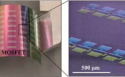
Bend me completely in grafenovski h4> For another group of South Korean scientists has proposed a method of creating graphene ultra-thin transistors again, ultra-thin polymer substrate consisting of a special epoxy resin.
First, an ordinary silicon substrate coated with a layer of silicon dioxide deposited thin layer of the polymer (SU-8) on which are already "print" graphene transistors, and then a layer of SiO 2 sub> simply dissolved, thereby separating thinnest film from the substrate. When this film can be transferred to virtually any surface, including the skin or tissue. The total thickness of the film - less than 100 nm!
The process of creating a thin film with ultra-thin MOSFETs i>
However, what problems await us when such a transfer? That's right, this is not uniform surface: bends, cracks, creases - everything that can be present on the tissue surface. After changing the geometry of the transistor, we thus changes its transport properties, including the mobility of the charge or the electric field distribution at the gate, that is, it turns out that at the same nominal voltage of the transistor in a bent condition begins suddenly pass a current, whereas in unstrained it will lock.
Fortunately, all these problems has been avoided as a result it was found that the position of the transistor (in the bend or on the flat surface of the tissue) is unimportant affects the electrical behavior of the transistor.
Testing of transistors with different arrangement of them i>
Anyway, like bends, stretching, folding the fabric in half:
Testing of transistors in bending, twisting and stretching i>
And without thinking twice, the scientists decided with the help of the developed technology to create a tactile sensor that can detect touch at 9 psi, which is equivalent to a pressure of 0.1 atmospheres or 100 grams force per cm 2 sup>:
The tactile sensor that can detect 0, 1 kgf / cm 2 sup> i>
This technology can be used in smart clothes, as no special equipment is required for the application (as they say, pasted and forgot), including, in part worn and no discomfort sensors heartbeat, oxygen level, and so on. But maybe - the devil Korean scientists are not joking - and help Biorobot bioprosthesis acquire tactile sensations.
Original article in ACSNano (DOI: 10.1021 / nn503446f) i> When will the first industrial graphene-based devices?
2 years to cope at least 3-5 years 5 years Never, graphene does not overcome the silicon lobby Only registered users can vote in polls. Sign , please. 109 people have voted. 17 people abstained. Will promising graphene-based LEDs without ITO (in displays, for example)? Yes, if the price is below the traditional with comparable characteristics Yes, even if the price is above the No, because of the low reliability No, because of the poor, "not enough" performance Only registered users can vote in polls. Sign , please. 75 people have voted. 37 people abstained. How do you treat a flexible and wearable electronics? I think this is good. Waiting for the implementation and will intensively use the I think this is good, but I will not use - I do not want to know Google and my pulse still < It is unlikely that we will see in the foreseeable progress in this area Absolutely waste of resources Only registered users can participate in the survey. Sign , please. 102 people have voted. 19 people abstained. Source: habrahabr.ru/post/234401/


Invented cheapest way water electrolysis
Physicians from Peking University first implanted person printed on the 3D-printer vertebra