1650
Silicon Electronics: bend me completely!
Today it seems that modern electronics, this is something monolithic, solid, but not far off that day and hour when the electronic device will be flexible (and some manufacturers have already succeeded!), Smart phones will be rolled-up and monitor a 2 meter will automatically "unroll" when you turn on the TV or computer ... This is, of course, until the dream, but a real flexible electronics already in all manufactured in laboratories worldwide as prototypes to find the most optimal and cheap technology.
Subject is not a flexible carbon, namely silicon electronics has prompted developers of the Institute of Science and Technology King Abdullah that Saudi Arabia (yes, oil is not a hindrance to progress), to develop a new method for transferring microelectronic components such as capacitance, transistors, and entire microarray on a flexible substrate of silica or polycrystalline / amorphous silicon.
Of course, the solution to this problem is not new and many laboratories have already done considerable work in this field. For example, IBM year ago unveiled his vision flexible electronics, before the mass was made attempts to create «подпружиненые »contacts , bonded to each individual, small chipy on conventional silicon conductive polymers and even decision based on carbon nanotubes , however described below technology requires only a small change in the production process technology and uses silicon and silicon dioxide.
So few people probably know that ordinary glass can be bent almost in half, the whole thing only in the thickness of the product. This is actually the same as comparing the aluminum or iron thin foil with a piece of metal surround. That presented technology uses this effect, i.e. the thickness of the substrate is reduced to only 5 microns. To separate the substrate from the carrier in it "drilled" a hole the size of about 3-5 microns, through which the reaction occurs and then etching the substrate with a uniform separation he carrier.
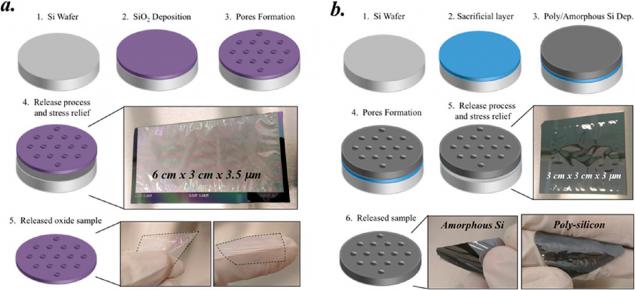
Two processes create flexible electronics: a) on a transparent substrate of silicon dioxide and b) on a conventional silicon substrate i>
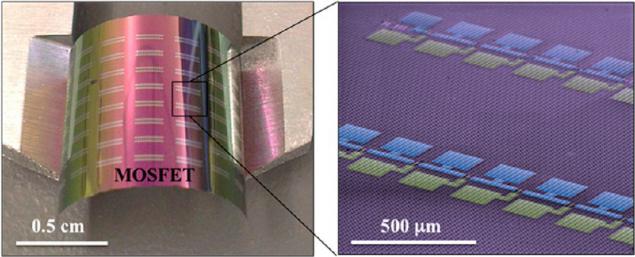
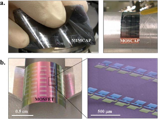
To test the efficiency and reproducibility of the manufacturing process, the authors have created a flexible semiconductor capacitance (MOSCAP), field effect transistors ( MOSFET ), and capacitors metal-insulator-metal (MIMCAP). All test samples confidently bend and show virtually indistinguishable performance compared with volumetric counterparts.
The capacitors and field-effect transistors by a thin and flexible plates of silicon i>
But that's not all, the work is presented in the same work ready devices such as micro-Li-Ion battery and a thermoelectric generator:

Demonstration of real devices: ab) thermoelectric generator and its characteristics ©, d) lithium battery and its capacity (e) i>
Speaking of cost, the authors write that all involved in the production processes are equivalent to those used on a normal production, except for one - reactive etching using XeF 2 sub> followed by separation of the plate. However, at 18 cm 2 sup> plate consumed about 2 g of this compound (100 cycles, 30 sec / cycle). Given the cost at $ 8 / g, it turns out that everything goes in the process of etching $ 0.88 / cm 2 sup>, which is not so little. A recovery of Xe - at least partly - will reduce costs many times over. In addition, the thinning of the substrate will significantly save materials.
And finally, a video in which the authors of the "game" with 4 inch wafers, which can take here .
Original article published in the journal ACSNano .
Source: habrahabr.ru/post/219211/