1096
All beam
This post I continue to use the theme of explosive electron emission, which I recently told in an article & quot; At the heart of the cathode spot & quot ;. The next interesting technology and equipment for the generation of low-energy high-current electron beams (LHEB) in an extended plasma channel. This technology enables production of surface alloys have a number of unique characteristics. On the practical application of this technology, its development prospects and unusual areas of application will be discussed in this article.
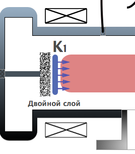
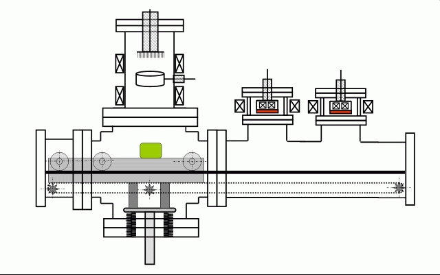
How does it work? B> h5> To generate the electron beam is necessary to use a vacuum chamber, in which there are cathode reflex discharge ( K1, K2 i>) and a plasma anode (< i> A i>). The distance between the cathodes 20-50 cm. The process takes place in a magnetic field. For the production of the plasma in the discharge gap to be an inert gas at low pressure. You can use different gases, but is more commonly used inexpensive argon.
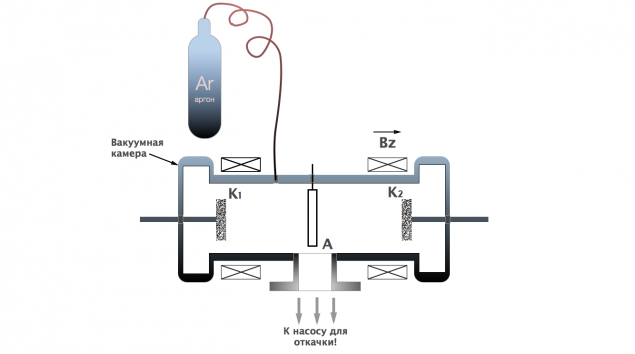
The pressure is not great - a few thousandths of a millimeter of mercury to maximize & quot; идеальности" gas. Thus, the mean free path of gas molecules at least an order of magnitude larger than the size of the discharge cell and is about ten meters.
Now, to light reflective discharge must be grounded cathodes K1, K2 i>, and from the switching power supply ( SP i>) to submit the momentum of the positive voltage to the anode. Also, do not forget to include a magnetic field. The scheme will now look like this, as shown in the figure.
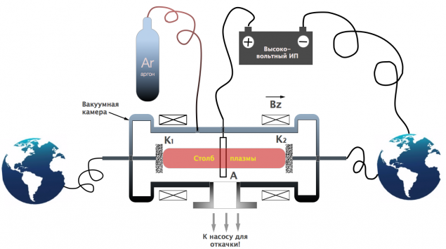
Suppose that between the cathode K1 i> and the anode And i> there was a free electron. The movement of electrons to the anode prevents the strong magnetic field that spins as it were in the discharge of his cell. Electrons start to oscillate between the cathodes causing ionization of the gas molecules. There are additional electrons, which in turn pick up and amplify the ionization process, which is starting to be an avalanche. The space between the cathode is filled with plasma, on their surfaces having катодные spots and discharge switches in high (arc) stage.
This discharge is called a reflection, as it occurs due to multiple reflection of electrons from the cathode K1 i> and R2 i> as a ping-pong. Physics reflective discharge well изучена. Sometimes, such a discharge is called Penning discharge.


Generate beam h5> So, we have learned to create a stable plasma column inside the vacuum chamber. The discharge will exist as long as the supply voltage is filed. But this is not so interesting. Let's try to generate a powerful electron beam. For this discharge pre-charged up to 30-50 kV capacitor to one of the cathode discharge cell.
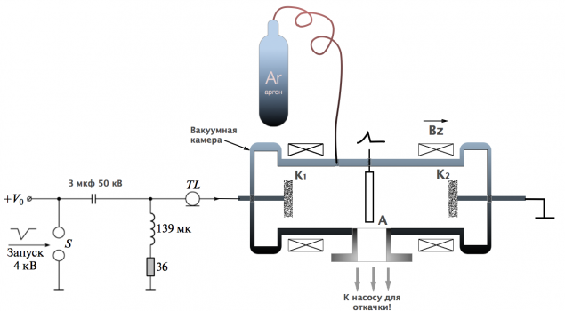
From the powerful DC voltage loads of high voltage capacitor. The charging circuit provides the coil. This is a very important element of the circuit! The inductor circuit provides all the work. In the constant current charging time of the capacitor its resistance is small (36 ohms) and capacitor discharge when there is a strong pulse of a few microseconds. Coil resistance increases sharply, and the entire energy stored in the capacitor is sent to the cathode K1 i>. The launch of the arrester circuit is S i>, which ignited a short control pulse of negative polarity in Q4. The energy transferred from the condenser at an agreed link TL i>, which is made of six parallel lines RC-50-9 cable of a certain length, to clearly agree on the load. All nodes of High Current Electronics serious. For example, a capacitor weighs more than 100 kg.
What happens at the time of high tension? At the cathode, a region of high negative charge, which is adjacent to the boundary of the plasma reflective discharge. There is a so-called double layer. This area is accelerating electrons which are emitted from the intense cathode spots.
Electrons get extra powerful acceleration. It begins the formation of the electron beam. The magnetic field continues to play an important role, not allowing the beam to collapse in a "cord." This provides a large aperture beam, and as a consequence - a decent area of the workpiece to 70 cm2. The pulse duration is 3-5 ms, the electron energy range 35-50 keV. The beam propagates in the anode plasma against the magnetic field and reaches the second electrode ( K2 i>), which is already in this case is called "collector". This is where we set any metal part that is subjected to the treatment. The plant operates continuously, with a frequency of 0.5 Hz. The frequency is determined by the power supply of the high-capacity capacitor and vacuum equipment. The whole setup is "wrapped" in a major automation and managed by a single operator. For the operation of the unit is written special software. In this introductory part shall be considered sufficient. It is better to talk more about the practical application of this technology.


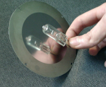
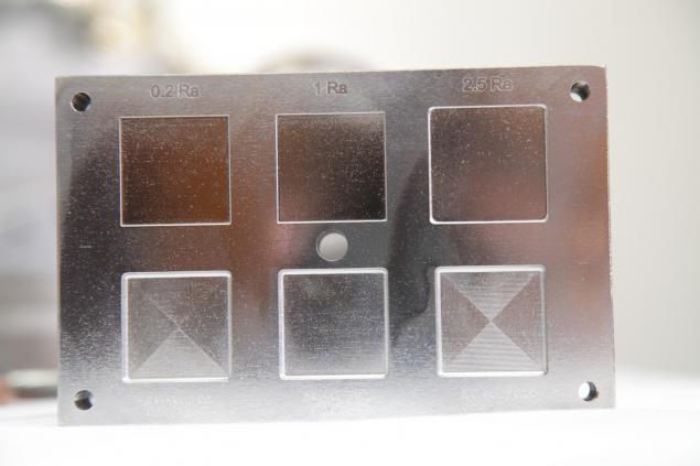
What happens to the surface of metal parts? B> h5> The electron beam melts a thin layer of the surface, creating a short time (millionths of a second) of the molten metal layer.
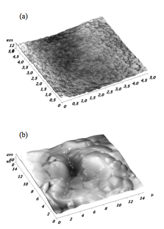
It occurs as the instantaneous heating of the metal and its fast cooling, which forms a new structure on the metal surface. There is a hardening of the surface, the dissolution of the different impurities, the formation of an ordered structure of the surface of the alloy. It is possible to adjust the characteristics of a wide range of the beam, creating the necessary framework for future surface ( in the figure - and - before treatment, b - after i>).

Application of Technology h5> The technology is widely used to increase the electrical strength of vacuum insulation. It is used for the manufacture of fuses, components and assemblies of microwave electronics, delaying structures, вакуумных switches, etc. On the one hand, the effect is achieved by cleaning the surface from various contaminants and impurities, and the other - is carried polishing surface electrodes.
Certainly one of the most important uses of this technology is a modification of metals and alloys to produce unique performance. You can handle the specialized cutters, drills, nozzles, blades of jet engines and more. Resource machined parts can be increased by tens and sometimes hundreds of times. Beam can handle the details of the most complex forms.
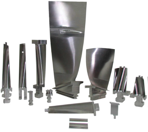
A very interesting application of the technology lies in the processing of molds. The surface of the mold is processed to modify the beam surface, which prolongs the service life of a mold (sometimes several times!) Or allows to produce a mold of a cheaper material.
This is especially true for molds working with corrosive materials or at elevated temperatures, for example, in the manufacture of glass. Details of molds is less subject to "fatigue" of the metal, as well as facilitated the process of breaking the mold.

A new direction, which gives additional opportunities for this technology - to create complex surface alloys, the receipt of which is not possible by any other means. For this purpose a beam to generate embedded magnetrons for sputtering different metals. This approach allows you to create nanostructured surfaces that have unique characteristics. It is resistant to aggressive environments, the highest strength while maintaining ductility and more. This processing occurs in one cycle without razvakuumirovaniya (magnetrons in figure shown on the right).
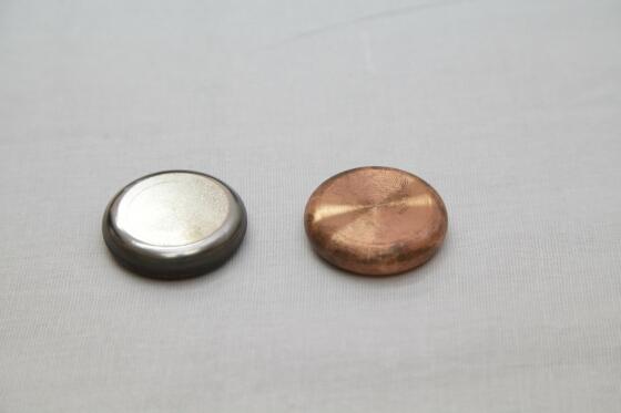
The technology allows you to create unique surface alloys with disinfectant properties. It noticed the Japanese and let men razor blades are processed by this technology. Also workpiece for dental crowns, medical tools and more. Application of the technology much!
In most cases, buyers of such equipment are foreigners. These are companies from Japan, China, the United States and European countries. Russian experts, unfortunately, only just eyeing such technologies.
I have been visiting the guys who make and promote this technology. A short video (5 minutes).
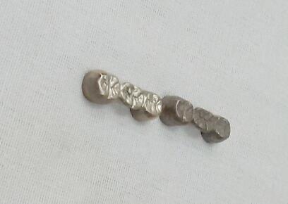
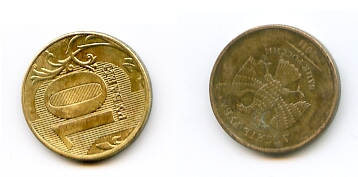
Coin after treatment process only the front side of the coin ("tails"). Processing in the soft state, as Russian coins with a thin coating.
I do not give a direct link to the Site does not violate the rules, but I want to help the children in their interesting project, so if you have any questions or interest in the practical applications of the technology - write in a personal or asmtomsk@gmail.com
Have a great day everyone!
Source: geektimes.ru/post/250492/


Stand Alone .....
Open pre-order the earliest Steam Controller, Steam Link and nektoroye types Steam Machines