In pursuit of a blue LED
Recently, Habré and Giktayms there were many informative articles about LED lamp , their circuitry and production . Development of the main components - the blue LED - took a quarter century, and the authors of the most successful technologies have been awarded this fall Nobel Prize . I would like to highlight this story from the physics and explain why the way to the blue diode was so long and thorny.
Introduction
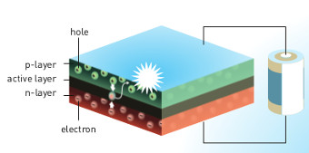
Habré has talked in detail about based on semiconductor electronics and about, How does the LED . Briefly recall the main points. If you apply for a pn junction forward voltage, electrons from the n-region and holes from the p-region will move towards each other and recombine, emitting energy in the form of photons.
Источник
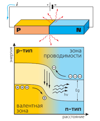
Now look at the band diagram. The applied voltage crosses the electrons in the conduction band (respectively, holes in the valence band). Met, they recombine.
Source i>
It can be seen that the energy of the emitted photons is approximately equal to the width of the band gap. Actually, it also determines the wavelength of light and color. Thus, the energy of the photons of blue light more than red - so for blue LEDs need a semiconductor with a wide band gap. Historically, these semiconductors are called wide band
Generally speaking, the semiconductors in the world is not so much, and their basic properties are well understood. Very instructive here is the schedule (Alferov in his Nobel lecture, calls it "world map" semiconductors):
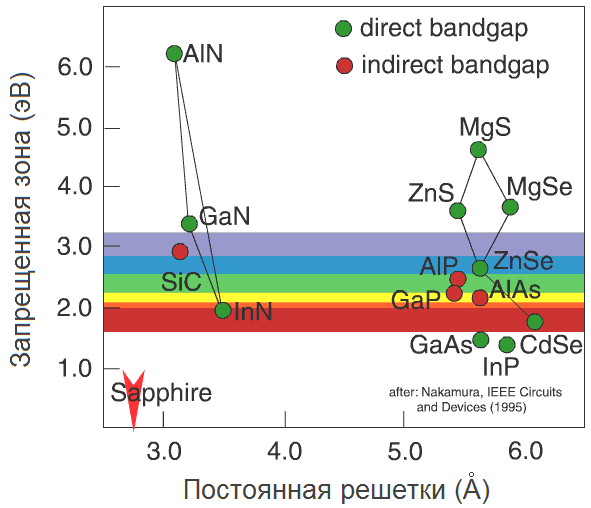
Horizontal here postponed lattice constant of a semiconductor - roughly the distance between two neighboring atoms in the crystal (to her we shall return later). Vertical - bandgap in electron volts (eV). To have an idea, one sees from photons with an energy of 1.8 eV (wavelength 700 nm, red) to 3.1 eV (400 nm, violet). We are interested in the blue-violet region, with a margin of about 2.6-3.3 eV it.
Digression: electron volts According to the definition, energy of 1 eV is sufficient to reduce the potential of an electron at 1 volt. Conversely, if we increase the potential of the electron at 1 Volt (say, after he could run from "-" to "+" odnovoltovoy batteries), he will receive the energy of 1 eV. Thus, if the band gap of the semiconductor is 3 eV (violet LED), then to throw an electron in the conduction band, you can increase its capacity at 3 V. In general, this is determined by the operating voltage on the LED, reaching as much as 3-3.5 In for blue / violet diodes.
As we can see, in the blue-violet region fall only three semiconductor: SiC, ZnSe and GaN. Historically, in the order they appeared on "LED" arena.
1. Silicon carbide (SiC)
Silicon carbide is remarkable in that it can form a huge amount of crystalline modifications. Already in the 50s is allowed to create structures with different band gaps - and thus generate radiation in different parts of the visible spectrum. After the red and yellow LEDs first blue LED was developed in 1969. In the '80s they became commercially available.
But for all the technological progress efficiency devices does not exceed 0.03%. The reason was fundamental. To understand it, we have to go a little further into physics.
direct-gap semiconductors and indirect- h5> In fact, the band structure of the semiconductor is a little more complicated than in the picture above. The position of the zones (and the band gap) depends on the pulse of an electron in a crystal (ie actually on its speed). Moreover, the vector depends not only on the magnitude and the direction. The result is something like this:
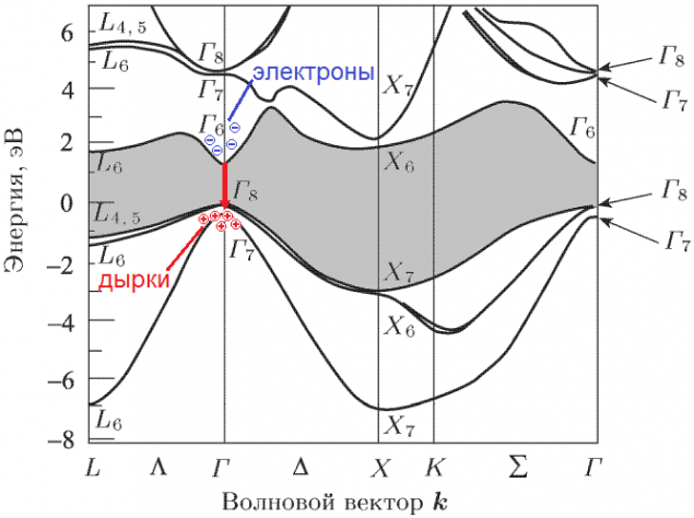
Source: [1] i>
This band structure of GaAs. Vertical traditionally deferred energy. Horizontal ¬- not going into details - shows the different possible values of the momentum vector (which is also called wave vector i> or position of the electron in the Brillouin zone i>). For example, the electrons in the gamma point (any of the letters in the image D) have zero momentum. Bandgap I paint it gray for clarity. Now look at the red arrow: an electron from the the lowest point i> of the conduction band falls in top point i> of the valence band without changing the pulse (the same coordinate horizontally), emitting a photon. This direct transition.
And what happens in the SiC?
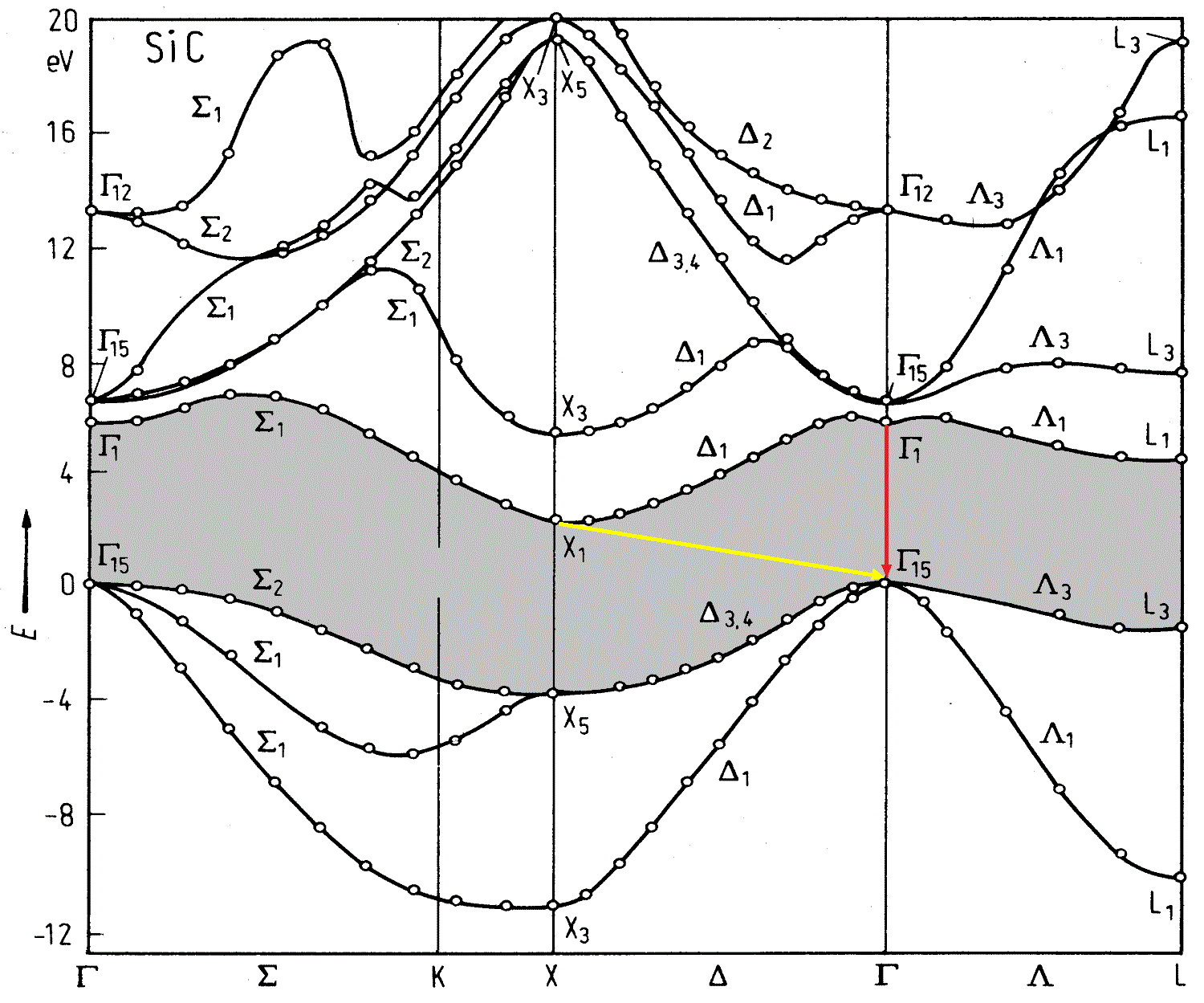
Source i>
We look at the yellow arrow. Electrons from the lowest point of the fall not vertically downwards, and at an angle ( Indirect Transfer) - then they change their momentum. The problem is that this momentum of the emitted photon is too large, and the law of conservation of momentum has not been canceled. Need another particle - phonon - able to compensate for the electron momentum. However, now our process of two-particle (electron - photon) was the three-particle, which significantly reduced his credibility. For the LED means that of all the electrons in the conduction band, only a few will be able to radiate a photon - which means we will lose much in the CAP.
Q: i> and the figure out the red arrow, it is all good?
A: i> Yes, the transition line, but its energy is about 6 eV (good ultraviolet eyes to burn, you can). For us, it's overkill.
Actually, it is an indirect transition SiC determined his fate (or rather its end) in optoelectronics. Fortunately, ZnSe and GaN were direct-gap semiconductors.
2. Zinc selenide (ZnSe)
ZnSe different from SiC not only intelligence and wit direct transition, but also the possibility of the growth of high quality structures on GaAs substrates widespread. It quickly became clear, however, and lack of material, be fatal.
Firstly, there was a problem with the manufacture of contact to the diode. Contact must be made of metal, and at the metal-semiconductor inevitably formed Schottky barrier i>. ZnSe trouble was that the barrier Schottky seen a huge drop in voltage. As a result, the operating voltage of the diode reaches 10 volts instead of the expected 2.8. Later, it was reduced to 4.2, and then only at the cost of complicating the tangible production.
The next problem was the heat. The low mobility of electrons in ZnSe is in a high resistance (and hence a large heat release); low thermal conductivity makes the situation even worse.
Finally, the most serious obstacle was the degradation of the material in the process. The essence of this process is reduced to a sharp increase in the number of defects in the crystal at high current densities or radiation. This wildly reduces the life of the device (in general, it is difficult to talk about the "lifetime" when the laser diode burns after 20 seconds of operation).
Thus, with a zinc selenide were only thin blue diodes. In stock had one material, the possibility of which first few believed.
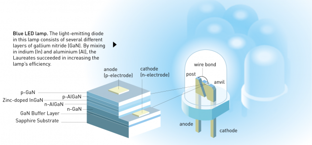
3. Gallium nitride (GaN) and other III-nitrides
To understand why a GaN diodes returned only in the mid-80s, you remember how generally produce LEDs. Thin layers of semiconductors (in fact, all the electronics harder transistor) grown epitaxial methods. The essence of the word is that we are deposited on the surface of the semiconductor atoms, which lie not piecemeal, but quite orderly - and repeating as if continuing up the crystal lattice. (This is simply energetically favorable.) As a result, layer by layer, we get an almost perfect crystal.
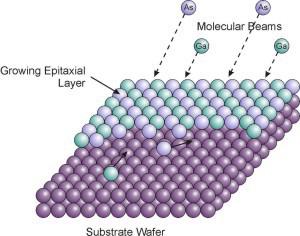
Source i>
The subtlety here is that we can not start from scratch epitaxy. Need an initial single crystal - substrate
Digression: Growth substrates Probably many readers Giktayms raised in childhood salt crystals. We had to tie a thread seed - grain of salt - and hang it in a salt solution. So, semiconductor single crystals grow at about the same - of course, of the components of the highest purity, while still rotating seeded and slowly pulling it upward. It is called Czochralski
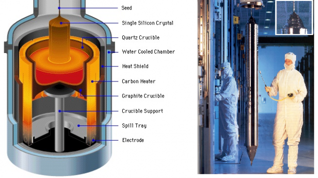
Source: 1 , 2 . i>
Further simple: take a substrate of silicon carbide epitaxy to grow on her carbide-silicon diode. Although there is a problem with the ZnSe: ZnSe substrate produced not so widely. Then let's take a GaAs substrate: according to the "world map" lattice constants of GaAs and ZnSe almost identical (5.66 Å), then growth will go well. The problem would be if we took a substrate of silicon carbide with a lattice constant of about 3 Å: ZnSe could not repeat such a close lattice due to internal stresses (in fact, the repulsion between the atoms of Zn and Se). Even on silicon (5.4 Å, a difference of 5%) to grow ZnSe would be problematic - from a certain layer of the internal stress in the ZnSe layer would be too great, and he wanted to grow up with his usual lattice constant. The transition from one grid to another would look something like this:
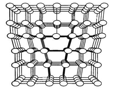
Источник
That is, the discordance lattices leads to just such defects. A defect in optoelectronics - this is very bad. Moral: to choose the right substrate for epitaxial!


Solid solutions h5> Take a ZnSe crystal and replace all the atoms of zinc magnesium atoms. Obtain crystals MgSe, which are slightly different lattice constant (a magnesium atom more zinc atom) and the band gap. And if not replace all of the atoms, but only some? Say, five percent? Get something intermediate: the shape of the crystal lattice will remain the same, but the lattice constant and band gap will be somewhere between onymi for ZnSe and MgSe. This substance is called solid solution ZnSe and MgSe, referred to as Zn 0.95 sub> Mg 0.05 sub> Se and "world map" is based on the straight line connecting the ZnSe and MgSe.
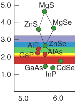
Actually, just on the "world map" shows which pairs of semiconductors, there are stable solid solutions. Thus, controlling the concentrations of the components with growth, we can adjust and the lattice constant and the band gap of the semiconductor - and thus control the wavelength of the radiation. Thus, the addition of indium in GaN allows us to go from ultraviolet (3.4 eV) in the visible blue region (2.7-2.9 eV).

The substrate for GaN h5> Now it is clear what is the value "world map": it allows to select the solid solutions for controlling the wavelength and related materials for the substrate. Well, let's pick up the substrate for the growth of InGaN (so happened that the GaN substrate to grow impossible). Wait, how it is - there are no suitable substrates? Not at all?
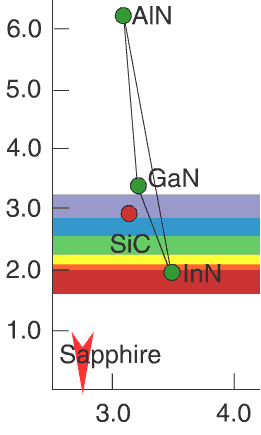
SiC is close, but not optimal (the difference between the lattice constants 4%) and to the same roads. Because of the price mainly used sapphire. I>
In fact, the absence of substrates was the reason that in the 80 years, worked with zinc selenide. It was believed that the quality of growth should be a key success factor. Virtually the only exception was a group of Isamu Akasaki at Nagoya University. By 1986, they offered a tricky solution. The essence was that were grown on a sapphire substrate, several intermediate (so-called buffer ) layers of GaN. The concentration of defects in them was huge, but decreased from layer to layer. Later, Shuji Nakamura (Nichia Corp.) perfected this process by using AlGaN buffer. Was such a structure:
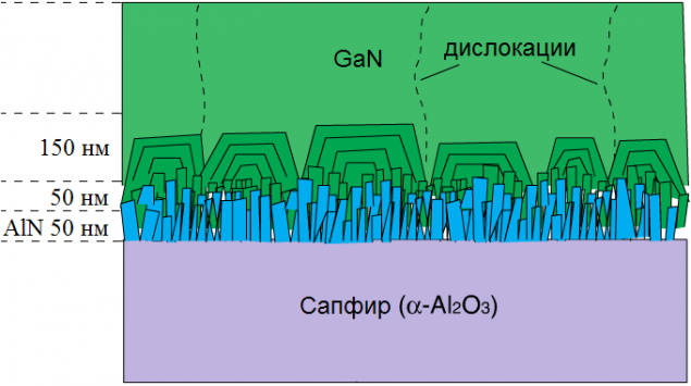
Source i>
In the electron microscope, it looked like this:
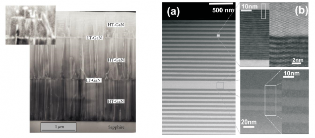
left - GaN on sapphire, the right to compare ZnSe on GaAs (GaAs substrate is not shown, but judging by the size of it close). Note the scale: GaN and a half times thicker. Sources: 1 , 2 . i>
Thus, even after all the improvements dislocation density remains enormous. A defect for optoelectronics - is not just bad, but really i> bad: they capture the great media and allow them to recombine nonradiatively, drastically reducing efficiency. This is the difference between the diode and LED: make a pn junction is not a problem, do flawless i> pn junction - a complex technological problem. For example, GaAs LED with defect concentration as in the picture obviously would not work (or rather, would, at best, but as a diode).
Here nature intervened: it turned out that the resulting quality is sufficient for normal operation of the LEDs. The reasons for this are extremely trivial and not studied until the end. One of them - not the usual mobility of carriers in GaN: they do not travel long distances and can therefore avoid the dislocation. Furthermore, virtually all of the dislocations in the GaN whiskers extending from the substrate to the surface of the diode. This imposes some restrictions on their properties that can be used in practice.
Unbelievable but true: the biggest problem of gallium nitride was suddenly behind.


acceptor in GaN h5> Another difficulty was the p-doping of gallium nitride. In the early stages as a acceptor (material for p-doping) used magnesium. However, the resulting material does not behave as a p-type semiconductor. There was some unknown factor that prevented Magnesium plays the role of acceptor.
The easiest way to determine the degree of doping - is to measure the resistance of the material. At the p- and n-doped semiconductors is low due to the excess carriers (electrons or holes in the n- to p-type). In a pure semiconductor free carriers is not, so the resistance is high. Blockquote> Notable next episode. Akasaka was able to show that irradiation GaN low-energy electron beam solves the problem: magnesium starts to behave as an acceptor . However, in the production of material again ceased to be conductive. This occurred during the annealing
Nakamura noted that the p-conductivity disappears at an annealing temperature above 400 ° C. At the same temperature to begin to dissociate the ammonium nitrogen and hydrogen. And what if the problem had something to do with hydrogen? Detailed studies have shown that Nakamura was right: atomic hydrogen penetrates the structure, was associated with magnesium and shared with him their electron without giving play the role of acceptor. Annealing in nitrogen instead of ammonium immediately solved the problem:
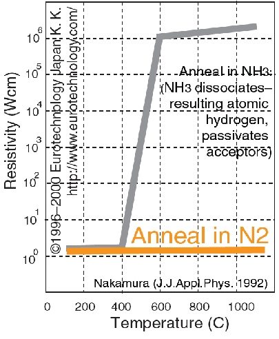
The upper curve: during annealing in Ammonium above 400 ° C the resistance of the material increases dramatically. In nitrogen (lower line) does not. Source. i>
Later it was found that annealing in nitrogen not only solves the problem of ammonium - it is able to completely replace the electron beam. That is, instead of what he was doing Akasaka, you can simply anneal in nitrogen material: it will destroy the connection with hydrogen and magnesium to make p-conductive material. Technologically, it was extremely important: processing of large crystals of electron beam - it is not cheap and not quick.
Happy end h5>
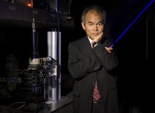
Shuji Nakamura. Источник.
The story is not over, but the main problems were solved. Along the way, managed to make a lot of interesting things, for example, to develop a special reactor for the growth of III-nitride. By 1994, Nichia Corp. commencement of commercial production of blue InGaN LEDs.
Sources
[1] P. Yu, M. Cardona "Fundamentals of Semiconductor Physics" - M .: FIZMATLIT, 2002. - 560 pp.
[2] S. Nakamura, S.Pearton, G. Fasol "The Blue Laser Diode: The Complete Story" - Springer, 2000. - 368 p.
[3] H. Morkoç et al. J. Appl. Phys. 76, 1363 (1994).
[4] http://www.eurotechnology.com/store/solidstatelighting/
[5] http://www.nobelprize.org/nobel_prizes/physics/laureates/2014/ (Hence the title picture, too)
Source: geektimes.ru/post/242961/