463
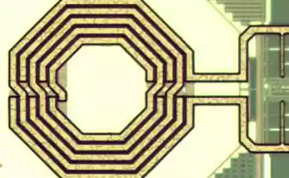
The finest in the world diamond films have a thickness of 30 nanometers

Siberian scientists have learned how to produce diamond films with a thickness of 30 nanometers. This is an order of magnitude thinner than is produced in Europe and the US.
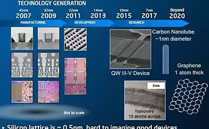
Head of the laboratory of the Institute of Semiconductor Physics (ISP) name Rzhanova Siberian Branch of Russian Academy of Sciences Vladimir Popov said in an interview that the smaller the chip thickness of the material, the less there is a parasitic effects and noise, less energy consumption, so nanofilms - an ideal base for chips. For example, a silicon film with a thickness of up to one nanometer, developed in the Institute of Semiconductor Physics, is used by organizations of Rosatom and the Russian Space Agency to create devices, radiation-resistant electronics; institutes of RAS and RAMS use them in nanoelectronic devices and biosensors.
Now the diamond film thickness of 300 nm is obtained in several laboratories around the world, but all their undoubted advantages are crossed so-called residual defects which are formed by separating the film from the crystal.
"We found a way to avoid the appearance of defects at all stages of the process and keep the original structure of the synthetic crystal which is grown by our colleagues from the Institute of Geology and Mineralogy SB RAS," - said Popov.
Using quantum optical effects in diamond chips on orders increase the amount of computation computers. In addition, diamond chips can operate at temperatures up to + 800 ° C, which, in particular, would allow the devices to create a direct control and adjustment of work and other jet engines.
The scientist also noted that Diamond could displace from the market of silicon microelectronics. But it will happen when will a technology that allows to make him the chip: it needs to grow a crystal with the desired properties, to learn how to peel off from his finest films and embedded into its crystal structure other chemical elements (doped) to enhance its low conductivity. < br />
Source: www.ria.ru
Innovation Center "Skolkovo" social networks VKontakte, Twitter, facebook and Google +
Site Facility: www.sk.ru
via factroom.ru