1509
Intel revealed plans to conquer 10 and 7 nm
Further development of microprocessors may require a non-silicon
4,654,288
theme of the International Conference on semiconductor circuits ( International Solid-State Circuits Conference ) in This year, sounded like a "small chips for big data." The event was held from 22 to 26 February in San Francisco, California, USA. Intel regularly participates in ISSCC, was no exception and 2015. Size for the Giants Intel and AMD is not unusual to make an important announcement there. Many reports told of internal investigations Intel, which touched on the potential for a real application of the technology, including further reduction of process technology chips. In particular, touched on this exciting topic of how to attack Moore's Law 10 nanometers.
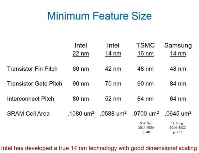
Intel is proud of the conquest of 14 nanometers. This achievement was given with difficulty and delays in 6-9 months, depending on the class of product, but the company still managed to achieve superior performance Samsung and TSMC. Intel believes that only they managed to achieve this 14 nm: talking about it smaller individual elements, and other characteristics, such as cell size SRAM.
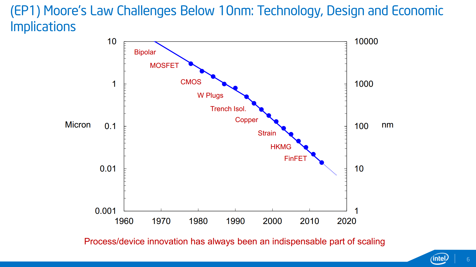
Intel predicts that the transition to 10nm will improve, but the specific timing of the deliveries was not called. If you focus on previous plans, the 10 nm will be released in late 2016 or early 2017. 10 nm and a further reduction will be given to very hard. Intel learns from his mistakes at work on 14 nm and hopes to avoid the same mistake when moving to 10.
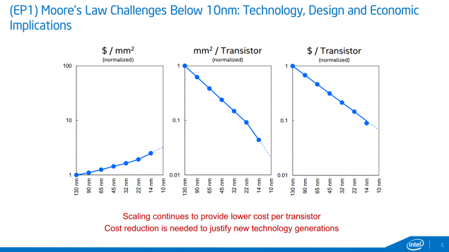
The question was also about the cost of the process. In the graph of Mark Bohr, you can see how the cheapening of individual elements. It can be seen that 14 nm showed a slightly larger decline in value than expected. This was achieved by optimizing the lithography process and the use of masks. And let 10 nm steps the use of masks will be even more delays that we have seen in the situation of 14 will not. Intel has realized that the delays were caused by the 14 nm increased number of tests and inspections. As a result, power correction PV test run 10 nanometers and a half times faster than in the case of 14 nm. Let the fixed costs will be higher than 10 nanometers, but the cost will fall to the transistor using the same techniques of lithography. Intel considers the глубокий UV , but does not want to use it unless absolutely necessary due to the slower process of its development than expected.

In addition, the research team talked about using Intel technology 3D (layer by layer) and 2.5D (individual layers on the substrate). These solutions can afford to fit more transistors: in some cases limit the power consumption (2.5D) or build more compact design (3D). In particular, Intel is considering scenarios in which the logic circuits of different production methods are stacked in layers instead of implementing such a single layer. This may appear in mobile devices - smartphones, tablets.

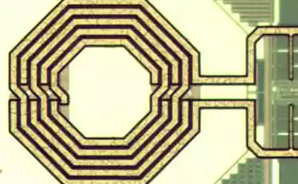
The most interesting development of technology 14 nanometers can be SRAM: Intel reached a 84-megabit storage with the world's smallest cell size - 0, 050 mkm². This 14 5 megabits per square millimeter. Compared to 22nm required voltage dropped 0, 1 to 6, 5 GHz, 1 to 3 GHz.
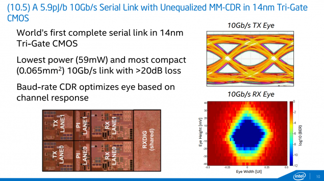
Intel achieved a very economic data: 10 Gbit / s required only 5, 9 pJ per bit em>

10 nanometers will require innovation and the transition to seven altogether will only be possible with new materials and processes. But nothing concrete has not been named, although discussed III-V semiconductors. This goes combinations of elements of the third group of the periodic table (aluminum, gallium, indium) from the fifth group elements (nitrogen, phosphorus, arsenic, antimony). The electron mobility in them is higher than that of silicon, which allows to reduce the size of transistors. In Intel начали look this way a few years ago, maybe in a few years will be the core of computer chip on Indium gallium arsenide.
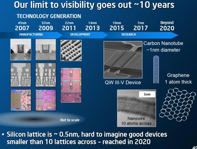
Further progress looks quite futuristic: possible deep ultraviolet, carbon nanotubes, graphene nanowires and em>
Based on materials Ars Technica , ExtremeTech and AnandTech.
Source: geektimes.ru/post/246676/
4,654,288
theme of the International Conference on semiconductor circuits ( International Solid-State Circuits Conference ) in This year, sounded like a "small chips for big data." The event was held from 22 to 26 February in San Francisco, California, USA. Intel regularly participates in ISSCC, was no exception and 2015. Size for the Giants Intel and AMD is not unusual to make an important announcement there. Many reports told of internal investigations Intel, which touched on the potential for a real application of the technology, including further reduction of process technology chips. In particular, touched on this exciting topic of how to attack Moore's Law 10 nanometers.
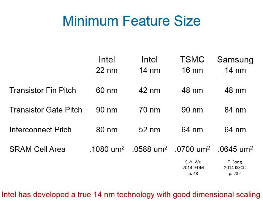
Intel is proud of the conquest of 14 nanometers. This achievement was given with difficulty and delays in 6-9 months, depending on the class of product, but the company still managed to achieve superior performance Samsung and TSMC. Intel believes that only they managed to achieve this 14 nm: talking about it smaller individual elements, and other characteristics, such as cell size SRAM.
Intel predicts that the transition to 10nm will improve, but the specific timing of the deliveries was not called. If you focus on previous plans, the 10 nm will be released in late 2016 or early 2017. 10 nm and a further reduction will be given to very hard. Intel learns from his mistakes at work on 14 nm and hopes to avoid the same mistake when moving to 10.

The question was also about the cost of the process. In the graph of Mark Bohr, you can see how the cheapening of individual elements. It can be seen that 14 nm showed a slightly larger decline in value than expected. This was achieved by optimizing the lithography process and the use of masks. And let 10 nm steps the use of masks will be even more delays that we have seen in the situation of 14 will not. Intel has realized that the delays were caused by the 14 nm increased number of tests and inspections. As a result, power correction PV test run 10 nanometers and a half times faster than in the case of 14 nm. Let the fixed costs will be higher than 10 nanometers, but the cost will fall to the transistor using the same techniques of lithography. Intel considers the глубокий UV , but does not want to use it unless absolutely necessary due to the slower process of its development than expected.
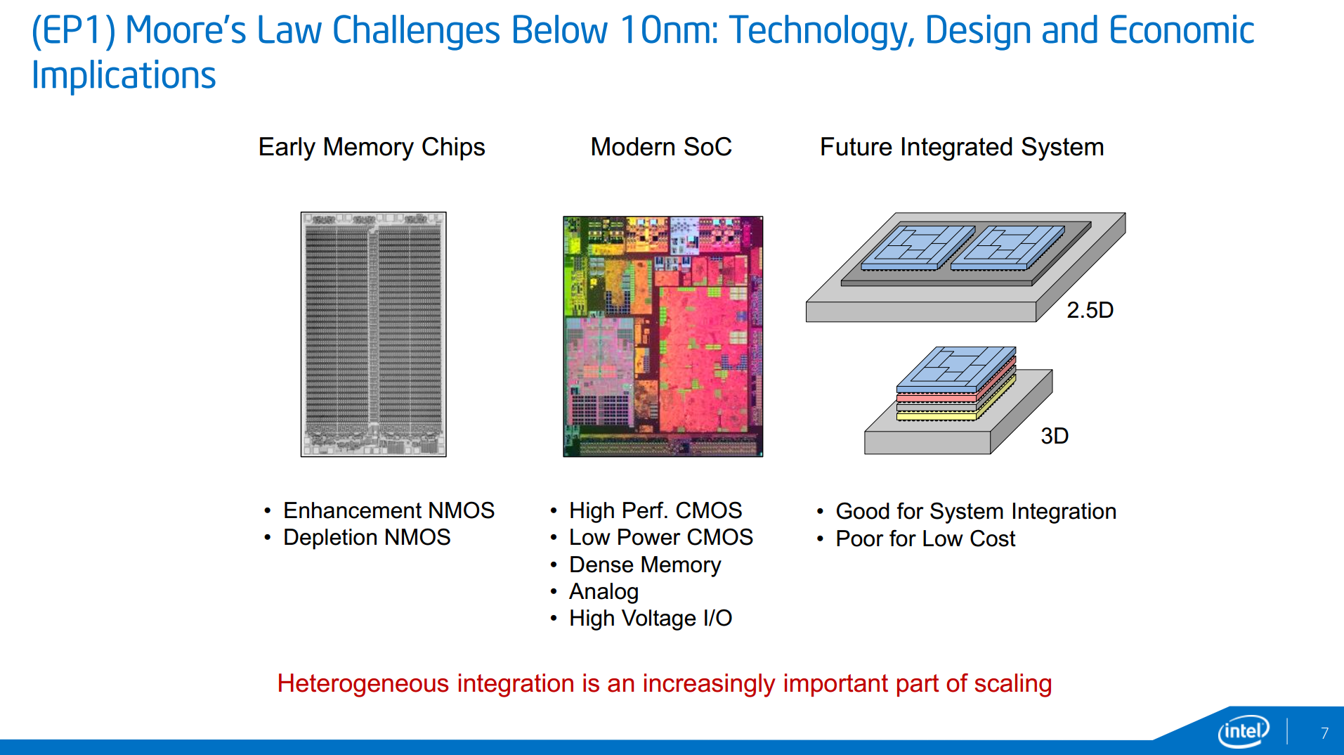
In addition, the research team talked about using Intel technology 3D (layer by layer) and 2.5D (individual layers on the substrate). These solutions can afford to fit more transistors: in some cases limit the power consumption (2.5D) or build more compact design (3D). In particular, Intel is considering scenarios in which the logic circuits of different production methods are stacked in layers instead of implementing such a single layer. This may appear in mobile devices - smartphones, tablets.
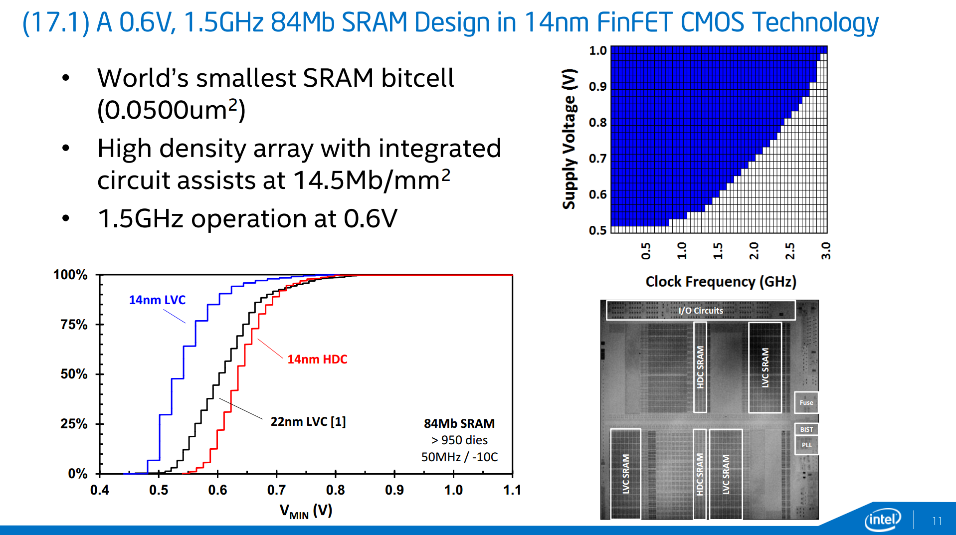
The most interesting development of technology 14 nanometers can be SRAM: Intel reached a 84-megabit storage with the world's smallest cell size - 0, 050 mkm². This 14 5 megabits per square millimeter. Compared to 22nm required voltage dropped 0, 1 to 6, 5 GHz, 1 to 3 GHz.

Intel achieved a very economic data: 10 Gbit / s required only 5, 9 pJ per bit em>
10 nanometers will require innovation and the transition to seven altogether will only be possible with new materials and processes. But nothing concrete has not been named, although discussed III-V semiconductors. This goes combinations of elements of the third group of the periodic table (aluminum, gallium, indium) from the fifth group elements (nitrogen, phosphorus, arsenic, antimony). The electron mobility in them is higher than that of silicon, which allows to reduce the size of transistors. In Intel начали look this way a few years ago, maybe in a few years will be the core of computer chip on Indium gallium arsenide.

Further progress looks quite futuristic: possible deep ultraviolet, carbon nanotubes, graphene nanowires and em>
Based on materials Ars Technica , ExtremeTech and AnandTech.
Source: geektimes.ru/post/246676/


The development of artificial intelligence game methods
Scientists got the image of light, which behaves like a wave and a particle at the same time