189
Multi-layer solar panels set record for light conversion efficiency
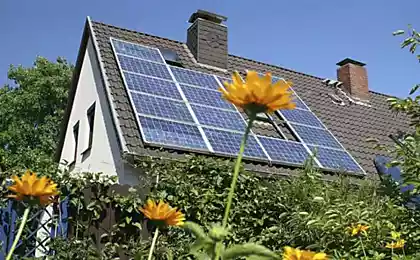
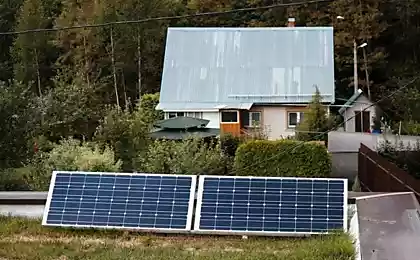
Engineers from the University of Illinois at Urbana-Champaign have developed a new type of solar panel in which photovoltaic cells are arranged in layers, instead of the traditional flat placement, which allows full use of the full spectrum of solar radiation.
The panels are capable of capturing radiation of different wavelengths, which has a positive effect on the conversion efficiency, which reaches a value of 44%, which is much higher than the 29% efficiency of standard solar panels.
The project is led by Professor John Rogers, who works with Semprius and Solar Junction.
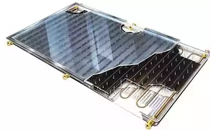
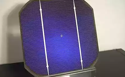
The team developed a way to use soft stamp printing to produce extremely small and thin layers of semiconductor material placed one above the other. The high-speed process provides a four-layer unit solar panel that enables the conversion of sunlight with a very wide spectrum coverage.
Semprius has combined the invention with its development – a two-stage optical system that can pinpoint an object a thousand times more light than hits it directly. Semiconductor materials are used for the three upper layers, while germanium is used for the lower layer.
For example, for the upper layer of an element, a material with a wide bandgap (forbidden zone, semiconductor characteristic) can be used that will absorb and convert high-energy photons, whereas the inner layers can be created from materials with a narrow bandgap and will absorb low-energy photons. These elements also have a highly efficient transparent inner layer that allows the resulting electrons and holes from adjacent layers to pass through the collector of the element without recombining.
A big challenge to further improve the technology of multilayer photovoltaic cells may be the accuracy of placing layers on the grid relative to each other, something that will be extremely difficult to achieve with further increase in the number of layers. Even more difficult, when using a traditional design, the outputs of each layer must be precisely the same because within the element they are connected in series.
Although the developers are trying to get around these difficulties using various techniques for connecting layers (for example, a physical connection or using various organic binders with anti-reflective properties), none of these methods has yet reached 100%. They give too much internal reflection, have low thermal conductivity characteristics or are destroyed by thermomechanical stress that occurs with large amounts of sunlight.
Developers don't despair. “We used our ideas and developments to produce photovoltaic cells with a conversion efficiency of 43.9% and an efficiency of 36.5% for an array of cells.” “While these figures have not yet been confirmed by external laboratories, these are the best numbers ever obtained for photovoltaic technology of any type,” Rogers said.
“We are currently using composite semiconductor materials for the top three layers and germanium for the bottom layer,” explains Scott Burroughs, vice president of technology at Semprius. “We measured the efficiency of both individual elements and arrays of them, combining them with high-performance optics in the laboratory and in the open sun.”
Now the team is working on developing the technology and obtaining five- and six-layer elements to further improve efficiency.
from nanotechweb.org
Source: facepla.net


Huge reserves of water found in the mantle of our planet
3D printer builds house in Amsterdam + video