1049
Green energy and nuclear silicon
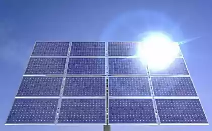
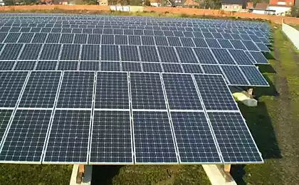
I think very few people are aware that the entire renewable energy industry today depends on the work of research reactors. It is about getting it nuclear-doped silicon (YALK), which is used for the production of high-power semiconductors, without which it is impossible RES. Now more.
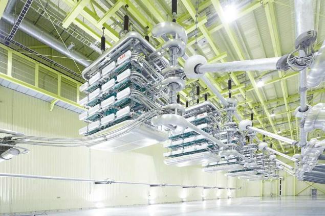
12-pulse rectifiers (hanging left) ultravysokovoltnyh power lines are also important consumers of nuclear-doped silicon. i>
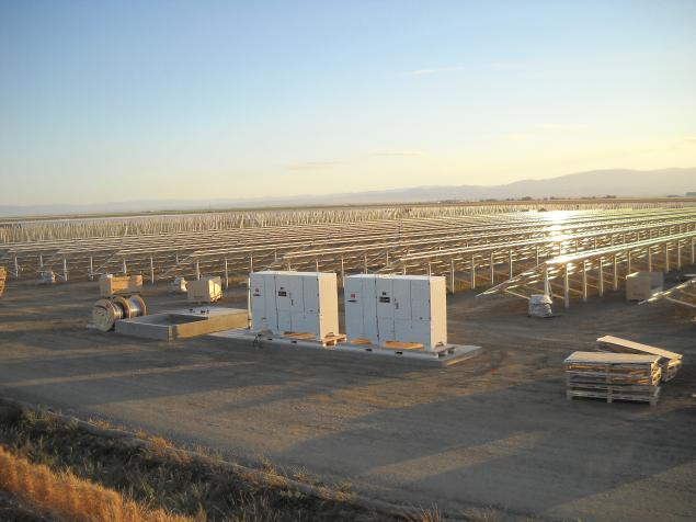
If we look at the diagram of any solar or wind power, make sure you see there inverter - electric machines that convert direct current to one another and network variables. They need to dynamically manage the flow of electricity within the SES or the windmill and docking with the global supply network in the correct mode.
These unattractive boxes convert megawatt DC voltage of several hundred volts in 50 hertz 10-35 kV. i>
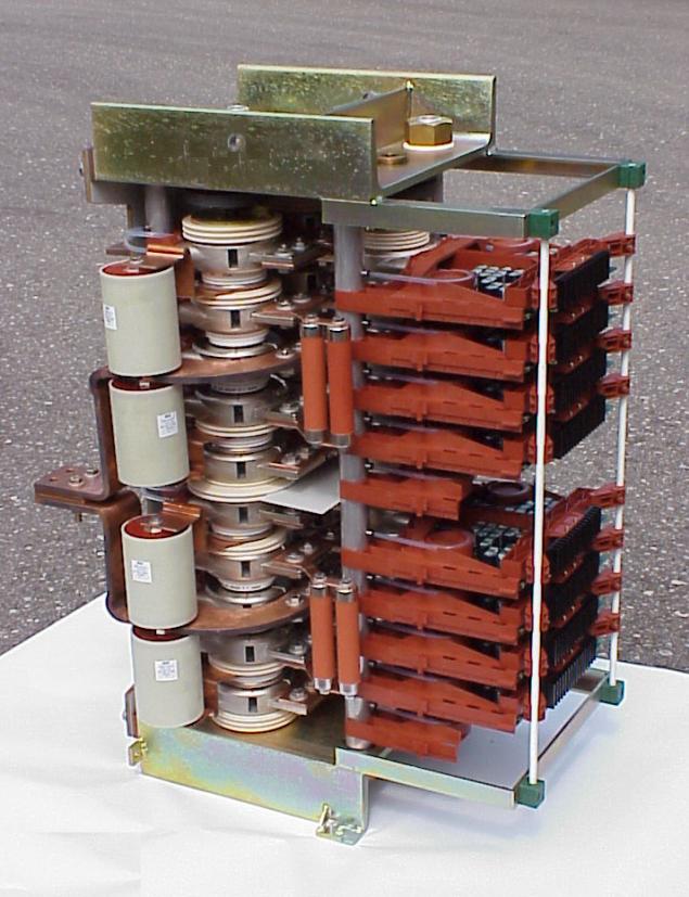
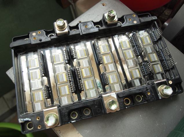
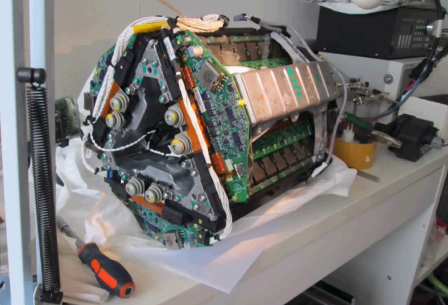
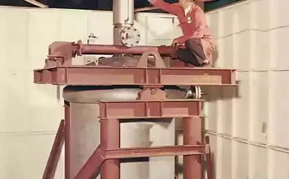
And inside them work here are the key assembly - it is such a single-phase H-bridge 6 MW, it is 8 IGCT thyristors, which are below. i>
Inverters in turn are collections of passive filters, inductors and transformers of workers and most importantly - powerful electric keys. The power inverters today employs two types of semiconductor switches - IGBT transistors and thyristors IGST (by the way the letter I in these devices represent entirely different :))
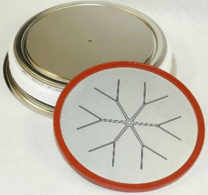
IGCT thyristor (tablet left) and manage the scheme (right). The thyristor is made of a circular silicon wafer i>
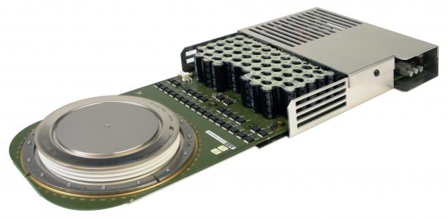
And the opened IGBT modules a little less power. There is no need for a high-current gate drive, and the key is assembled from many small crystals i>
Relatively small semiconductor switches today have maximum operating voltages up to 7000 volts at an operating current of 5000 A, ie the size of a tea saucer capable of switching 35 megawatts. Along with the highest efficiency in the region of 99% and a relatively high switching frequency such keys largely determined world of modern power electronics. Today, in addition to renewable energy and power lines ultra-high voltage direct current, the main consumer of such products are actuators (motors) with high efficiency and flexible work - such as electric drives, electric vehicles and Tesla high performance machine tools.
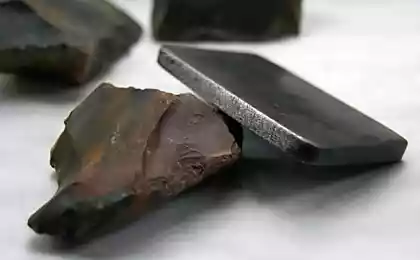
The thyristor in the body (the so-called press-pack) and the actual silicon wafer, which commutes the current. i>
So, all the semiconductor switches with operating voltages above 1600 volts are made of silicon, which has been irradiated in a nuclear reactor - nuclear-doped silicon. Currently, about 150 tonnes of silicon in this year receive two dozen irradiators, usually on the basis of research reactors. Manufacturers are scattered around the world, and the volume of the market - about 150 million dollars a year, and this is one of the biggest world market of isotope products. Including several Russian research reactors (Tomsk Polytechnic University, Karpov, Lighthouse, RIAR) provide about 10% of world supply. Typically, the organization owning the reactor is operated in conjunction with the providers of silicon, which prepare the raw material, and provide a breaker bars on the plate and marketing.
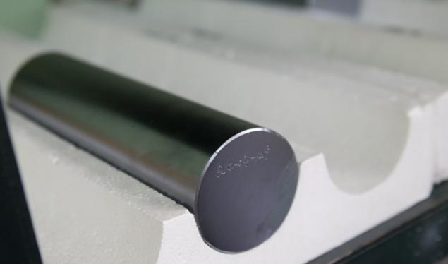
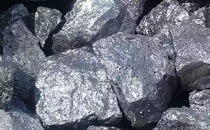
The ingot after irradiation and annealing. i>
Nuclear-doped silicon (or Neutron transmutation doped silicon) is an ultra-pure silicon, in which the neutron radiation of the reactor part of the atoms of the isotope 30Si transmuted into phosphorus atoms 31P, creating doped n-type conductivity. Traditionally, such a doping is created by mixing a very small amount of phosphorus in the silicon melt, but the problem is that while local ANALYSIS OF dopant may differ by tens of percent of the mean. The high voltage switch such variation leads to the appearance of "hot spots" where starts to flow much more current than the national average and the transistor or thyristor breaks. Doping by neutron irradiation allows through some tweaks to achieve uniformity of better than 5% deviation from the average - sometimes better than 3%.
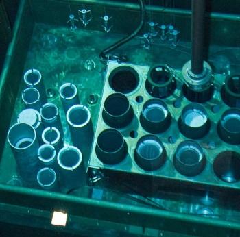
This irradiation device Danish company Topsil, which first took YALK commercial production at the end of the '70s. i>
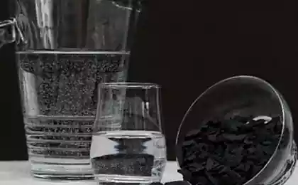
To do this, the ingot of pure single crystal silicon placed in a nuclear reactor, possibly shielded from gamma radiation and fast neutrons that damage the crystal structure. For standard values of the neutron flux research reactors (10 12 sup> to the 10 14 sup> neutron per cm 2 sup> per second) is required from a couple of hours to days of exposure To obtain a predetermined conductivity of the silicon crystal. This doping takes place by the reaction of 30 sup> Si + n - & gt; 31 sup> Si - & gt; 31 sup> P (half-life 2.6 hours), and the resulting Silicon is necessary to keep a couple of days, what would its radioactivity has fallen to safe levels.
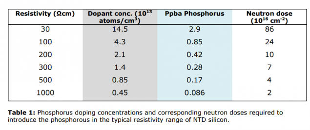
The relationship between the neutron dose, conductivity and get the content of the dopant in YALK i>
During irradiation bar rotate and move up and down for uniform illumination of neutrons. In addition to some powerful reactors used profiling absorber cadmium or boron, which further smoothes uneven axial neutron flux.
However, today there are non-nuclear methods of doping silicon, which allows to obtain almost nuclear quality, and they are being squeezed out of the field YALK 600-1600 volts, which previously was used only as a nuclear silicon. However, the higher the voltage is still not subject to chemical methods, and within the general trend to increase specific power voltage power electronics is constantly going up, so that the place has YALK silicon.
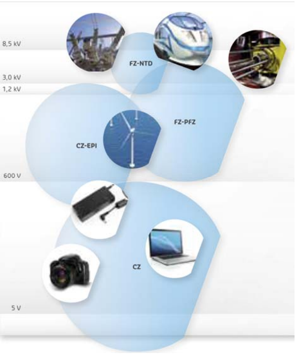
Other technology for doped silicon wafers (CZ, CZ-EPI, FZ-PFZ and nuclear FZ-NTD) focused on different niches, including voltage, the picture from the leading manufacturer of silicon Topsil i>
Moreover, analysts predict the growth of consumption YALK associated with an increase in the number of electric vehicles with high-voltage battery (when the battery voltage is 800 volts are already used keys with an operating voltage of 1600 volts or higher, based on the Yal silicon). Some estimates say about the growth of the market from 150 to 500 tons and above in the next decade. Therefore, many newly built reactors at the design stage lay the channels to obtain nuclear doped silicon, hoping thereby to reduce the cost to taxpayers of the reactor. For example, such channels will be MBIR and JHR .
But while the inverter Tesla Model S managing 300 kilowatt engine incorporates 84 IGBT transistor with an operating voltage of 600 volts it is likely not related to nuclear-doped silicon. However, this is not the most advanced solution available today. i>
So the "green electric future" of humanity is inextricably linked to nuclear technology, nuclear reactors and other environmentally unfriendly horrible legacy of the 20th century.
Source: geektimes.ru/post/268882/

12-pulse rectifiers (hanging left) ultravysokovoltnyh power lines are also important consumers of nuclear-doped silicon. i>
If we look at the diagram of any solar or wind power, make sure you see there inverter - electric machines that convert direct current to one another and network variables. They need to dynamically manage the flow of electricity within the SES or the windmill and docking with the global supply network in the correct mode.

These unattractive boxes convert megawatt DC voltage of several hundred volts in 50 hertz 10-35 kV. i>

And inside them work here are the key assembly - it is such a single-phase H-bridge 6 MW, it is 8 IGCT thyristors, which are below. i>
Inverters in turn are collections of passive filters, inductors and transformers of workers and most importantly - powerful electric keys. The power inverters today employs two types of semiconductor switches - IGBT transistors and thyristors IGST (by the way the letter I in these devices represent entirely different :))

IGCT thyristor (tablet left) and manage the scheme (right). The thyristor is made of a circular silicon wafer i>

And the opened IGBT modules a little less power. There is no need for a high-current gate drive, and the key is assembled from many small crystals i>
Relatively small semiconductor switches today have maximum operating voltages up to 7000 volts at an operating current of 5000 A, ie the size of a tea saucer capable of switching 35 megawatts. Along with the highest efficiency in the region of 99% and a relatively high switching frequency such keys largely determined world of modern power electronics. Today, in addition to renewable energy and power lines ultra-high voltage direct current, the main consumer of such products are actuators (motors) with high efficiency and flexible work - such as electric drives, electric vehicles and Tesla high performance machine tools.

The thyristor in the body (the so-called press-pack) and the actual silicon wafer, which commutes the current. i>
So, all the semiconductor switches with operating voltages above 1600 volts are made of silicon, which has been irradiated in a nuclear reactor - nuclear-doped silicon. Currently, about 150 tonnes of silicon in this year receive two dozen irradiators, usually on the basis of research reactors. Manufacturers are scattered around the world, and the volume of the market - about 150 million dollars a year, and this is one of the biggest world market of isotope products. Including several Russian research reactors (Tomsk Polytechnic University, Karpov, Lighthouse, RIAR) provide about 10% of world supply. Typically, the organization owning the reactor is operated in conjunction with the providers of silicon, which prepare the raw material, and provide a breaker bars on the plate and marketing.

The ingot after irradiation and annealing. i>
Nuclear-doped silicon (or Neutron transmutation doped silicon) is an ultra-pure silicon, in which the neutron radiation of the reactor part of the atoms of the isotope 30Si transmuted into phosphorus atoms 31P, creating doped n-type conductivity. Traditionally, such a doping is created by mixing a very small amount of phosphorus in the silicon melt, but the problem is that while local ANALYSIS OF dopant may differ by tens of percent of the mean. The high voltage switch such variation leads to the appearance of "hot spots" where starts to flow much more current than the national average and the transistor or thyristor breaks. Doping by neutron irradiation allows through some tweaks to achieve uniformity of better than 5% deviation from the average - sometimes better than 3%.

This irradiation device Danish company Topsil, which first took YALK commercial production at the end of the '70s. i>
To do this, the ingot of pure single crystal silicon placed in a nuclear reactor, possibly shielded from gamma radiation and fast neutrons that damage the crystal structure. For standard values of the neutron flux research reactors (10 12 sup> to the 10 14 sup> neutron per cm 2 sup> per second) is required from a couple of hours to days of exposure To obtain a predetermined conductivity of the silicon crystal. This doping takes place by the reaction of 30 sup> Si + n - & gt; 31 sup> Si - & gt; 31 sup> P (half-life 2.6 hours), and the resulting Silicon is necessary to keep a couple of days, what would its radioactivity has fallen to safe levels.

The relationship between the neutron dose, conductivity and get the content of the dopant in YALK i>
During irradiation bar rotate and move up and down for uniform illumination of neutrons. In addition to some powerful reactors used profiling absorber cadmium or boron, which further smoothes uneven axial neutron flux.
However, today there are non-nuclear methods of doping silicon, which allows to obtain almost nuclear quality, and they are being squeezed out of the field YALK 600-1600 volts, which previously was used only as a nuclear silicon. However, the higher the voltage is still not subject to chemical methods, and within the general trend to increase specific power voltage power electronics is constantly going up, so that the place has YALK silicon.

Other technology for doped silicon wafers (CZ, CZ-EPI, FZ-PFZ and nuclear FZ-NTD) focused on different niches, including voltage, the picture from the leading manufacturer of silicon Topsil i>
Moreover, analysts predict the growth of consumption YALK associated with an increase in the number of electric vehicles with high-voltage battery (when the battery voltage is 800 volts are already used keys with an operating voltage of 1600 volts or higher, based on the Yal silicon). Some estimates say about the growth of the market from 150 to 500 tons and above in the next decade. Therefore, many newly built reactors at the design stage lay the channels to obtain nuclear doped silicon, hoping thereby to reduce the cost to taxpayers of the reactor. For example, such channels will be MBIR and JHR .

But while the inverter Tesla Model S managing 300 kilowatt engine incorporates 84 IGBT transistor with an operating voltage of 600 volts it is likely not related to nuclear-doped silicon. However, this is not the most advanced solution available today. i>
So the "green electric future" of humanity is inextricably linked to nuclear technology, nuclear reactors and other environmentally unfriendly horrible legacy of the 20th century.
Source: geektimes.ru/post/268882/


Pictures at an Exhibition. Meet the first unmanned drone taxi EHang 184
Love the implementation of heat: