1376
Subtleties of microelectronic production
Many probably more than once wondered why processors, graphics cards and motherboards that we buy in stores - designed and made anywhere but not in Russia? Why is it, really, we can only oil pump?
How much is the production start-chip, and why in the presence of 22 nm factory, most chips around the world still is on "outdated" 180nm-500 nm equipment?
How does the production of microelectronic and how much it is worth?
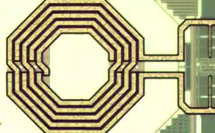
Transistors are drawn on the wafer by photolithography using devices called steppers or scanners. Stepper - draws a frame (up to 26x33mm) entirely, then moves to a new position. Scanner - simultaneously and shifts the mask plate so that at every moment only one narrow draw "row" in the center of the frame, thus the aberration of the optical system is less affected by the image. Main characteristics steppers / scanners - the wavelength of light, which they work (for mercury lamps i-line - 365nm, then the excimer laser - 248nm and 193nm), and the numerical aperture of the lens. The shorter the wavelength, and the larger the aperture - the smaller details can be drawn lens in accordance with the diffraction limit:

For example, one of the most advanced scanners ASML NXT 1950i with a wavelength of 193nm and a numerical aperture of 1.35, and k1 = 0.4 (normal value for photolithography no "tricks"), we obtain the theoretical resolution of 57nm. Applying tricks like phase masks, multiple exposure, the optical proximity correction, off-axis illumination, the light polarization - get up to 22 nm minimal elements.
Other options steppers / scanners - performance (how many plates per hour they can process up to 220 plates), and alignment error (how many nanometers in pieces misses the positioning of the plate relative to a given position. In modern scanners - to 3-5nm).
Steppers / scanners print reduced by 4-5 times the image here is a mask (a glass plate with a picture chip size approximately 15x15sm) in precisely defined locations.
Printing operation pattern (with different masks) must be repeated by ~ 10 (for the most simple and old chips) to ~ 40 times to form all the layers on the chip (starting from the transistors themselves, and ending with 2-10 layers of metal compounds). Between operations photolithography plates subjected to various treatments - warm them in the oven to 1100 degrees, etched in a solution and plasma. The output remains plate cut into individual crystals, and placed in a test housing.
"Coolness" technology measures the size of the minimum of the drawn elements (parts of the transistor, such as the shutter - can be either smaller or larger than this figure - that is the amount sufficient conditional). It is clear that the smaller transistors - the faster the chip, and more crystals will fit on the plate (but not always need the maximum speed).
Now begins the slow and painful transition to EUV-lithography with a wavelength of 13.5nm and mirror optics. EUV scanners while more expensive and slower than usual 193nm, and just starting to surpass them achievable resolution.
How much is your processor do?
Figures - rough estimates, accurate nowhere say without NDA.
Software license per workstation Developer chips - from 20,000 to 100,000 dollars a year or more. It is certainly possible and steal, but behind this all around the track.
Next - making masks. They should not have any damage, and their production is very expensive: from ~ $ 7'000 per set for chips at 1000nm ~ $ 100,000 for chips at 180nm and up to ~ $ 5'000'000 for chips to 32nm . But the chip from the first time probably will not work - and after finding errors masks have to redo it. Partially this problem can be dealt with by placing the test chips to many customers on the same set of masks - then everyone will get a little bit of test chips for 1 / 3-1 / 10 price complete set of masks (this is called the Shuttle or MPW - multi project wafer).
Each plate is produced is from $ 100-400 for older technologies at 1000nm ~ $ 1000 at 180nm and up to ~ $ 5000 for the most modern (apart from nanometers here has an impact and complexity of technology - simple logic cheaper flash memory is more expensive, but at times ). Here it is also important to remember and about the size of plates: the most modern production are now working with a diameter of 300 mm plates - they are about twice the area of 200mm wafers (which are now used in Russia at Micron, integrals, and in the dim future Angstrom-T), and the last about twice as many more older 150mm. Plate large size allows you to obtain lower-cost chips for large orders as number of gestures for the manufacture of plates 100 is approximately the same, regardless of the diameter (it's one of the reasons the planned transition to advanced manufacturing 450mm wafers in 2018 according to optimistic estimates).
Suppose we want to develop a x86-compatible processor (or any other relatively complex chip) on a more or less modern technology commercially available 28 / 32nm (22nm though there but commercial orders until the place - so that access to technology is sometimes as love: money is not for sale). Question to the cost of patents omitted, it is generally a very sad topic. Suppose you need to develop a mythical 200 person-years (this is if we make a modest processor and not intended in the first place).
Licenses for software - 50k $ * 100 = $ 5 million (rough estimate, not everyone needs a license).
Salary developers - say 3k $ * 1, 5 (taxes) * 12 * 200 = 10.8 million $
Test run in MPW - 2 * 1.5 million $
Making masks for mass production of 2 * 5 million = $ 10 million $ (2 - because no matter how hard you try - the first time will come)
Total - 28.8 million $
It was what is called Non-recurring engineering (NRE) - one-time costs that do not depend on the volume of production, and the success of the event.
If the processor we have turned the area of 200mm2, plate technology 32nm diameter 300mm worth $ 5000, then we would get the plate 70690/200 = 350 crystals (upper bound), of which the work will say 300. That is, the cost of the crystal - 16.6, $ 20 after korpusirovki. How much is now such a processor can be sold? $ 50? $ 100? Subtract taxes and mark-up shops ...
And now the question - how much to sell such processors to recoup our NRE, interest on loans, taxes, and so forth? Million? 5 million? And the main question - is there any guarantee that these 5 million processors will be able to sell, given that the competition does not cost anything to produce 5 million more have their finished product?
Here is such a hell of a business turns out - huge capital expenditures, huge risks and reasonable profit at best.
China - solved the problem on their own way, they decided to put all school computers with the processors and Linux - and the problem is solved with the volume of production ((1) (2)).
Thus, the main question when creating chips - it's not how and where to produce, and how to develop and who then sell millions of units of the resulting product? And how much does it cost to build a factory?
The cost of modern plant gets to around $ 5 billion or more. Such a sum is obtained because the cost of licenses and other fixed costs are not strongly dependent on the volume of production - and advantageous to have large production to cost "smeared out" over large volumes of production. And every modern scanner (which actually draws these details 22-32nm) costs $ 60-100mln (the large factory there may be a couple dozen). In principle, 5mlrd - not so much money on a national scale. But of course, no one will spend 5 billion without a clear plan for the return on investment. And is there such a situation - despite the complexity of the industry, only work with an apparent monopoly profit (TSMC, Intel, Samsung and a few others), others could hardly make ends meet.
It just does not fit in my head - how is it to invest billions, and hardly to beat them? It turned out everything is simple - worldwide microelectronics cruelly subsidized industry - plants constantly begging for tax exemption and tax credits and dumping (in China have gone even further - SMIC plant was built at public expense, and then they "manage" - they call it Reverse Build-Operate-Transfer). After the appearance of each new technology (45nm, 32nm, ...) - the first plants monopolists have her and cut the basic income, and those who come to 2-5-10 years after the start - to work virtually at cost. As a result, earn money here is extremely difficult (without monopoly and without subsidies).
It seems to have realized in Russia - and large projects microelectronic plants has been postponed, and build small production - to lose money and if you lose them a little. And even 3,000 wafers per month, produced on Micron - a head covering consumption volume of tickets and defense Underground (subway ticket crystal has a size of 0.6x0.6mm, one 200mm wafer is obtained 87'000 tickets in the subway - but about the sad history with tickets Metro I'll discuss in a future article).
Contrary to popular belief, the special restrictions on the sale of equipment for microelectronics in Russia is not - Jackson - Vanik amendment to the US presidential moratorium is imposed annually, and only need to receive a regular export permit. Sami equipment manufacturers have a vested interest to make more money, and kick themselves for their part permits. But of course, no money no one does anything. So for your money - every whim.
But we must remember that your plant does not guarantee the full independence of production, and cheaper production abroad: the main cost is the technology / licenses and the cost of purchased equipment - and if their technology and equipment is not, and all import - and then get cheaper can not. Many supplies in any case have to be imported. Separate sore point - the production of masks, only very large factories may have "his" production of masks.
And how many nanometers need to be happy?
Many people think - that is, from Intel-and 22nm, 90nm and we - we are hopelessly behind, post a tractor ... But there is another side to the coin: look for example at the same motherboard: there are hundreds of semiconductor devices - MOSFET-s, drivers, chip supply any supporting detail - almost all of them lack the technology and 1000nm. All industrial electronics and integrated circuits for space and military - is almost 100% of the 180nm technology and thicker. Thus, the latest technologies are needed only for CPUs (which makes very difficult / expensive because of the high risks and high threshold to market), and various "zhopogreek" (iPhones, etc.). If something goes War, and Russia will lose import - without "zhopogreek" can live, but without the industrial, aerospace and military electronics - no. Ie in fact, we see that things are critical for the country as much as possible done in Russia (or buy in store), and then, without which it will be possible to live in extreme cases - import.
There are other factors - the same cost of masks. If we need to make a simple chip, do something for its production on 32nm mask worth $ 5 million - may be beneficial if this chip then produce a circulation of tens and hundreds of millions of copies. And if we need to just 100,000 chips - more profitable to save on masks and produce chip at the "thick" technology. In addition, the chip has pads, which are connected to the terminals of chips - to reduce them nowhere, and consequently, if the chip area comparable to the area of contact pads - something to do on a thinner chip technology also does not make sense (unless of course "thick norm" meet the requirements speed and power consumption).
As a result - the vast majority of chips in the world is done by "thick" technologies (350-500nm and thicker), and billions of chips leaving for export to the Russian plants (though mostly in the form of plates) - quite a demand and sold (so that the parent cards and cell phones have our chips and power transistors - but under foreign names).
Finally, the US F-22 Raptor, until recently flew on a processor Intel 960mx, developed in 1984, production in the US was then the norms 1000-1500nm - one much buzzed about what the Americans put in backward aircraft electronics (though, okay, a little buzzed). The main fact is not nanometers, and the correspondence of the final product terms of reference.
Summary
Market economy elves and microelectronic manufacturing - weakly compatible things. The more dig - the less you can see the market, more subsidies, cartels, patent restrictions, and other joys of the "free market." Business in this industry - is one big headache, with huge risks permanent crisis of overproduction and profit only monopolists.
It is not surprising that in Russia are trying to have a small, but its production to maintain independence, to lose less money. Neither of which arrived on the market conditions can not speak.
Well, not all chips have to 22-32nm production, the vast majority of the more profitable to produce chips on older 180-500nm equipment because of the cost of masks and production volumes.
Source
Source: http: //
How much is the production start-chip, and why in the presence of 22 nm factory, most chips around the world still is on "outdated" 180nm-500 nm equipment?
How does the production of microelectronic and how much it is worth?
Transistors are drawn on the wafer by photolithography using devices called steppers or scanners. Stepper - draws a frame (up to 26x33mm) entirely, then moves to a new position. Scanner - simultaneously and shifts the mask plate so that at every moment only one narrow draw "row" in the center of the frame, thus the aberration of the optical system is less affected by the image. Main characteristics steppers / scanners - the wavelength of light, which they work (for mercury lamps i-line - 365nm, then the excimer laser - 248nm and 193nm), and the numerical aperture of the lens. The shorter the wavelength, and the larger the aperture - the smaller details can be drawn lens in accordance with the diffraction limit:

For example, one of the most advanced scanners ASML NXT 1950i with a wavelength of 193nm and a numerical aperture of 1.35, and k1 = 0.4 (normal value for photolithography no "tricks"), we obtain the theoretical resolution of 57nm. Applying tricks like phase masks, multiple exposure, the optical proximity correction, off-axis illumination, the light polarization - get up to 22 nm minimal elements.
Other options steppers / scanners - performance (how many plates per hour they can process up to 220 plates), and alignment error (how many nanometers in pieces misses the positioning of the plate relative to a given position. In modern scanners - to 3-5nm).
Steppers / scanners print reduced by 4-5 times the image here is a mask (a glass plate with a picture chip size approximately 15x15sm) in precisely defined locations.

Printing operation pattern (with different masks) must be repeated by ~ 10 (for the most simple and old chips) to ~ 40 times to form all the layers on the chip (starting from the transistors themselves, and ending with 2-10 layers of metal compounds). Between operations photolithography plates subjected to various treatments - warm them in the oven to 1100 degrees, etched in a solution and plasma. The output remains plate cut into individual crystals, and placed in a test housing.
"Coolness" technology measures the size of the minimum of the drawn elements (parts of the transistor, such as the shutter - can be either smaller or larger than this figure - that is the amount sufficient conditional). It is clear that the smaller transistors - the faster the chip, and more crystals will fit on the plate (but not always need the maximum speed).
Now begins the slow and painful transition to EUV-lithography with a wavelength of 13.5nm and mirror optics. EUV scanners while more expensive and slower than usual 193nm, and just starting to surpass them achievable resolution.
How much is your processor do?
Figures - rough estimates, accurate nowhere say without NDA.
Software license per workstation Developer chips - from 20,000 to 100,000 dollars a year or more. It is certainly possible and steal, but behind this all around the track.
Next - making masks. They should not have any damage, and their production is very expensive: from ~ $ 7'000 per set for chips at 1000nm ~ $ 100,000 for chips at 180nm and up to ~ $ 5'000'000 for chips to 32nm . But the chip from the first time probably will not work - and after finding errors masks have to redo it. Partially this problem can be dealt with by placing the test chips to many customers on the same set of masks - then everyone will get a little bit of test chips for 1 / 3-1 / 10 price complete set of masks (this is called the Shuttle or MPW - multi project wafer).
Each plate is produced is from $ 100-400 for older technologies at 1000nm ~ $ 1000 at 180nm and up to ~ $ 5000 for the most modern (apart from nanometers here has an impact and complexity of technology - simple logic cheaper flash memory is more expensive, but at times ). Here it is also important to remember and about the size of plates: the most modern production are now working with a diameter of 300 mm plates - they are about twice the area of 200mm wafers (which are now used in Russia at Micron, integrals, and in the dim future Angstrom-T), and the last about twice as many more older 150mm. Plate large size allows you to obtain lower-cost chips for large orders as number of gestures for the manufacture of plates 100 is approximately the same, regardless of the diameter (it's one of the reasons the planned transition to advanced manufacturing 450mm wafers in 2018 according to optimistic estimates).
Suppose we want to develop a x86-compatible processor (or any other relatively complex chip) on a more or less modern technology commercially available 28 / 32nm (22nm though there but commercial orders until the place - so that access to technology is sometimes as love: money is not for sale). Question to the cost of patents omitted, it is generally a very sad topic. Suppose you need to develop a mythical 200 person-years (this is if we make a modest processor and not intended in the first place).
Licenses for software - 50k $ * 100 = $ 5 million (rough estimate, not everyone needs a license).
Salary developers - say 3k $ * 1, 5 (taxes) * 12 * 200 = 10.8 million $
Test run in MPW - 2 * 1.5 million $
Making masks for mass production of 2 * 5 million = $ 10 million $ (2 - because no matter how hard you try - the first time will come)
Total - 28.8 million $
It was what is called Non-recurring engineering (NRE) - one-time costs that do not depend on the volume of production, and the success of the event.
If the processor we have turned the area of 200mm2, plate technology 32nm diameter 300mm worth $ 5000, then we would get the plate 70690/200 = 350 crystals (upper bound), of which the work will say 300. That is, the cost of the crystal - 16.6, $ 20 after korpusirovki. How much is now such a processor can be sold? $ 50? $ 100? Subtract taxes and mark-up shops ...
And now the question - how much to sell such processors to recoup our NRE, interest on loans, taxes, and so forth? Million? 5 million? And the main question - is there any guarantee that these 5 million processors will be able to sell, given that the competition does not cost anything to produce 5 million more have their finished product?
Here is such a hell of a business turns out - huge capital expenditures, huge risks and reasonable profit at best.
China - solved the problem on their own way, they decided to put all school computers with the processors and Linux - and the problem is solved with the volume of production ((1) (2)).
Thus, the main question when creating chips - it's not how and where to produce, and how to develop and who then sell millions of units of the resulting product? And how much does it cost to build a factory?
The cost of modern plant gets to around $ 5 billion or more. Such a sum is obtained because the cost of licenses and other fixed costs are not strongly dependent on the volume of production - and advantageous to have large production to cost "smeared out" over large volumes of production. And every modern scanner (which actually draws these details 22-32nm) costs $ 60-100mln (the large factory there may be a couple dozen). In principle, 5mlrd - not so much money on a national scale. But of course, no one will spend 5 billion without a clear plan for the return on investment. And is there such a situation - despite the complexity of the industry, only work with an apparent monopoly profit (TSMC, Intel, Samsung and a few others), others could hardly make ends meet.
It just does not fit in my head - how is it to invest billions, and hardly to beat them? It turned out everything is simple - worldwide microelectronics cruelly subsidized industry - plants constantly begging for tax exemption and tax credits and dumping (in China have gone even further - SMIC plant was built at public expense, and then they "manage" - they call it Reverse Build-Operate-Transfer). After the appearance of each new technology (45nm, 32nm, ...) - the first plants monopolists have her and cut the basic income, and those who come to 2-5-10 years after the start - to work virtually at cost. As a result, earn money here is extremely difficult (without monopoly and without subsidies).
It seems to have realized in Russia - and large projects microelectronic plants has been postponed, and build small production - to lose money and if you lose them a little. And even 3,000 wafers per month, produced on Micron - a head covering consumption volume of tickets and defense Underground (subway ticket crystal has a size of 0.6x0.6mm, one 200mm wafer is obtained 87'000 tickets in the subway - but about the sad history with tickets Metro I'll discuss in a future article).
Contrary to popular belief, the special restrictions on the sale of equipment for microelectronics in Russia is not - Jackson - Vanik amendment to the US presidential moratorium is imposed annually, and only need to receive a regular export permit. Sami equipment manufacturers have a vested interest to make more money, and kick themselves for their part permits. But of course, no money no one does anything. So for your money - every whim.
But we must remember that your plant does not guarantee the full independence of production, and cheaper production abroad: the main cost is the technology / licenses and the cost of purchased equipment - and if their technology and equipment is not, and all import - and then get cheaper can not. Many supplies in any case have to be imported. Separate sore point - the production of masks, only very large factories may have "his" production of masks.
And how many nanometers need to be happy?
Many people think - that is, from Intel-and 22nm, 90nm and we - we are hopelessly behind, post a tractor ... But there is another side to the coin: look for example at the same motherboard: there are hundreds of semiconductor devices - MOSFET-s, drivers, chip supply any supporting detail - almost all of them lack the technology and 1000nm. All industrial electronics and integrated circuits for space and military - is almost 100% of the 180nm technology and thicker. Thus, the latest technologies are needed only for CPUs (which makes very difficult / expensive because of the high risks and high threshold to market), and various "zhopogreek" (iPhones, etc.). If something goes War, and Russia will lose import - without "zhopogreek" can live, but without the industrial, aerospace and military electronics - no. Ie in fact, we see that things are critical for the country as much as possible done in Russia (or buy in store), and then, without which it will be possible to live in extreme cases - import.
There are other factors - the same cost of masks. If we need to make a simple chip, do something for its production on 32nm mask worth $ 5 million - may be beneficial if this chip then produce a circulation of tens and hundreds of millions of copies. And if we need to just 100,000 chips - more profitable to save on masks and produce chip at the "thick" technology. In addition, the chip has pads, which are connected to the terminals of chips - to reduce them nowhere, and consequently, if the chip area comparable to the area of contact pads - something to do on a thinner chip technology also does not make sense (unless of course "thick norm" meet the requirements speed and power consumption).
As a result - the vast majority of chips in the world is done by "thick" technologies (350-500nm and thicker), and billions of chips leaving for export to the Russian plants (though mostly in the form of plates) - quite a demand and sold (so that the parent cards and cell phones have our chips and power transistors - but under foreign names).
Finally, the US F-22 Raptor, until recently flew on a processor Intel 960mx, developed in 1984, production in the US was then the norms 1000-1500nm - one much buzzed about what the Americans put in backward aircraft electronics (though, okay, a little buzzed). The main fact is not nanometers, and the correspondence of the final product terms of reference.
Summary
Market economy elves and microelectronic manufacturing - weakly compatible things. The more dig - the less you can see the market, more subsidies, cartels, patent restrictions, and other joys of the "free market." Business in this industry - is one big headache, with huge risks permanent crisis of overproduction and profit only monopolists.
It is not surprising that in Russia are trying to have a small, but its production to maintain independence, to lose less money. Neither of which arrived on the market conditions can not speak.
Well, not all chips have to 22-32nm production, the vast majority of the more profitable to produce chips on older 180-500nm equipment because of the cost of masks and production volumes.
Source
Source: http: //