1178
Scientists from IBM found interesting physical phenomenon on the example of "nanowires" of semiconductors
Nowadays miniaturization - one of the main factors responsible for the technical progress. In fact, currently used in computing the conductors, the thickness of which is thousands of times smaller than the thickness of a human hair. Thanks to a vanishingly small size, it is possible to create powerful, productive small size chips capable of doing something that has not been able to compute nodes of previous years, occupying entire rooms.
Now being actively developed technology for transmitting data by means of light signals within a single chip. This is possible by combining optical elements with semiconductors, graphene and carbon nanotubes, when the whole system is placed on a substrate of silicon.
Data transmission system using this typically means converting the light into electrical signals, and vice versa. For converting a first type of material commonly used Group III-V semiconductors which emit light. Well, for the inverse transform light into electricity using silicon and germanium.
A team of scientists from IBM found interesting physical phenomena which may lead to the fact that in the future the same material as is used for emitting light and for converting it into electricity within a single chip.
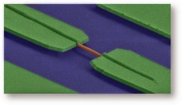
The journal Nature Communications recently was опубликована Article scientists Zurich units IBM Research. The article dealt with the fact that "nanowires" of the semiconductor can serve as an efficient light emitters and photodetectors effective. And to change the substance of the status of "radiation" in a state of "detecting" need to mechanical stress.
"When you stretch the entire length of nanowires, the material goes into what we call" controlled energy gap "(direct bandgap), in which he effectively emits light. But when you squeeze the wire along the axis of its electronic properties are changed, the material ceases to emit light. This state we call "psevdopryamym" (pseudo-direct), in this state materials III-V group behave like germanium or silicon photodetectors and become good, "- says the discovery of one of the researchers, Giorgio Signorello.
"These unusual properties are due to the fact that the atoms are arranged in a very specific such Explorer. We call this crystal structure, "Wurtz" (Wurtzite). This structure appears only in the ultra-small size conductors. You will not be able to achieve the same properties of the material with dimensions that are visible to the eye. This is a great example of the power of nanotechnology, "- says the first scientist colleague, Heike Riel.
As mentioned above, a similar phenomenon may open up the possibility of creating devices for optical transmission, where the same material is used for light emission and for its detection.
And that means new achievements, new breakthroughs in this field.
Via rdmag + ibmresearchnews
Source: habrahabr.ru/company/ibm/blog/220451/