761
One hundred percent Handmade electronics for beginners
The article describes some stages of hand-made electronic devices, and especially in detail about the first stage: the manufacture of printed circuit boards. Detailed photos of the process will help to understand the details. And the "dessert", to consolidate the theoretical material, we will assemble a simple electronic piano integrated timer NE555.
Prologue
We are all consumers of electronic devices: phones, tablets, televisions, etc. But only one in a thousand has some understanding of how it all works "from the inside", and to create an electronic design from scratch with your own hands can really only be elected. We offer you to join the exclusive club. Read this material, and, if you're interested, try your hand at the exploration of man-made electronics!
Those of you who find the strength to read the article to the end, can proudly declare itself "I understand something in electronics manufacturing," and that he who commits a feat and overpower the Assembly of the proposed design, it is worthy the title of "real electronics-Profi" (well, almost).
This master class is based on a set of Master kit NN201, which includes the details and materials necessary for the manufacture of printed circuit boards and electronic piano. Of course, if you want all materials and tools can be purchased alone, only have to spend time searching and purchase of the necessary components.
The necessary theoretical minimum
Any electronic design contains dozens, or even hundreds or thousands of components: resistors, capacitors, diodes, chips, etc. All of these components have a certain way of electrically and mechanically interconnected.
The most simple circuits can be soldered "on a knee" - point wiring, but this construction turns out ugly, confusing, has a questionable mechanical rigidity. Therefore, in any serious electronic design must be something like a chassis on which are mounted all of the parts. In different years the chassis was made from metal, cardboard or plywood, but in the last 20-30 years technological standard chassis is a printed circuit Board.
A printed circuit Board is a sheet of dielectric material, the surface of which the specific configuration of the applied strip of conductive material (usually foil). As the basis is most often used glass fiber: it is incombustible and possesses high dielectric properties, and low cost. In fiberglass drilled holes in which pass the findings of the parts. On the reverse side of the Board insights are soldered to copper current-carrying conductors that are configured a certain way. Soldering is carried out thanks to the mechanical fixing of the components to the Board, and thanks to the copper conductive tracks of the conclusions of parts electrically connected to each other.
Of course, the copper track conductors in the appropriate places to stick the Board to the fiberglass. But technologically easier to do the opposite: take a sheet of the PCB is glued with a continuous layer of foil and remove the foil from unwanted places.
Remove the foil from the unnecessary areas is possible by mechanical means: by making a sharp knife cuts in necessary areas. However, this method is time-consuming, traumatic, and is suitable primarily for the most simple of the schemes.
The foil can be removed and the chemical method: it is sufficient to immerse the Board into the solution, corroding copper (usually is a ferric chloride solution). Only beforehand it is necessary to protect from exposure to solvent those portions of copper (future current-carrying conductors) that need to be saved. As such protective equipment is sometimes used varnish, but easier to draw paths with a special marker. Also in practice electronics, widespread so-called laser-crystal cabochons technology (LUT). In this method, the pattern of future current-carrying conductors printed on a laser printer on special paper. Then the paper is applied to the blank fiberglass and iron this "sandwich" and iron: as a result, toner particles remain on the workpiece and subsequently will not be pretreated with a solvent.
The process of removing the foil is called etching. Etching is continued depending on the concentration and temperature of the solution is from several minutes to hours. After the process fee was washed with water and removed the protective structure, which shall remain copper conductors.
Then is drilling holes for the components. Usually used microdrile and drill diameter of 0.8 to 1 mm. Copper oxidizes rapidly in the air, and this complicates soldering. Therefore, immediately before soldering, the cost should at least be cleaned with fine sandpaper, removing a layer of oxides. But it is best to cover copper conductors with a protective composition, a layer of solder. This process is called tinning and it helps to maintain the high degree of suitability of the Board for soldering for several years.
In a production environment on top of the conductive paths is applied to a so-called solder – mask-layer protective material. This layer protects the conducting paths from accidental short circuits and damage. Only the pads remain free from the mask that makes it easy to produce their ration.
Another fabrication process – silk-screen printing – it involves the application in the "front" side of the Board with a special paint symbols and inscriptions. It makes life easier for installers of the Board and its repair.
But in the home to carry out the processes of applying a solder mask and silkscreen is difficult, so we will not do this.
All PCBs are ready. After that, the cost of all the components are mounted and then soldered. Then, the resulting structure is configured and tested. In modern factories, most of these processes are industrial robots, but humans, so all going to do with their hands.
The long-awaited practice
Much more interesting to do not just boring printed circuit Board, and a fee on the basis of which it is possible to collect practically useful device. We will make a simple electronic musical instrument – a toy piano with 8 keys.
Materials and components that we need:
— processing of fiberglass foil with dimensions of no less than 10x15 cm;
— a marker (preferably varnish) or nail Polish to protect the conductive tracks (the token can be found in stationery shops and nail to borrow from mom/girlfriend/wife);
— ferric chloride – powder weighing 100 grams will be enough for the eye.
— drill and drill bits with a diameter of 0.8, 1.0 and 1.2 mm;
non — metallic tub (deep bowl) – it must fit our billet. Better to find some old unwanted capacity, because after our experiments, it probably will have to throw it away or continue to use for etching;
— rubber gloves to protect our hands from the solution.
Note that the kit Master kit includes the billet NN201 with the already drilled holes, special pen and a beautiful red jar of ferric chloride weighing 100g. The set comes in a plastic blister, which serves as a great tray for etching!
For soldering you need:
— soldering iron, pliers, solder, flux;
— radio, a list of which is given below.
All you need can be found in stores radios or household goods.
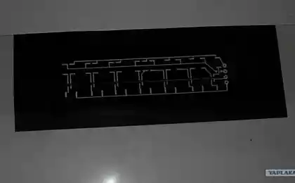
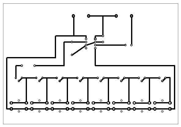
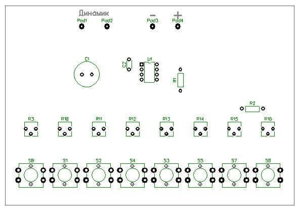
Schema-location pattern of current-carrying conductors of the printed circuit Board (looking from the side of the foil):
Preparing the PCB for etching
We clean the charge from the layer of copper fine-grained sandpaper (in the extreme case, suitable for rough ink eraser) and degrease with alcohol or gasoline;
Apply the template to the circuit Board and drill in the necessary holes;
Apply marker pattern of conductors and pads for the soldering of details, focusing on the wiring diagram and drilled holes, being careful not too much "slap" hands foil (so it is advisable to work in cotton gloves). In case of errors the marker is easily washed off with an alcohol solution. The dimensions of the contact pads under insights, you can do more (where space allows).
It is convenient to apply the drawings with a ruler, in two layers. After printing it is necessary to give the Board dry for about 10 minutes, then inspect the Board and correct any errors to finish, where the layer is thin, and procrasti with an awl or a thick needle seat incorrect merge tracks or pads.
Preparation of solutions and precautions
You must now prepare a solution of ferric chloride. For this purpose 100 grams of ferric chloride necessary to stir around 200-250 grams (one Cup) of warm water. Do not have to measure everything exactly to the gram: the process will go and at a slightly different ratio of ferric chloride and water, it is only necessary to note that the concentration of the solution and its temperature depends on the time of etching the Board.
In preparing the solution it is necessary to observe basic safety rules:
Etching the Board
Board is now ready for mounting and soldering components.
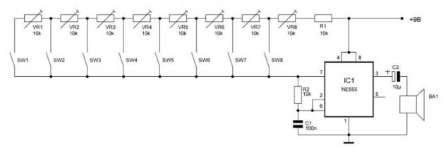
Description of the scheme
Consider the circuit of our design.
The scheme is built on the basis of the known chip NE555. IC chip included in a classic oscillator circuit whose frequency is determined by the capacitance C1 and the resistance between terminal "2" IC and "+" supply. When you press the buttons SW1...SW8 in customizados circuit chip includes a different potentiometer, respectively, BA1 speaker makes sounds of different pitch. As a result, even on such a basic musical instrument can play simple melodies.
Tool adjustment is made by trimming resistors VR1...VR8.
Circuit diagram:
Wiring diagram (side view detail):
We need the following details, which can be purchased at the hardware store; all these parts are included in the set NN201:
IC1 (IC chip) 1 PCs NE555P C1 (electrolytic capacitor) 10 UF 1 EA. C2 (ceramic capacitor) 0.1 µf 1 PC R1, R2 (resistors) 10K 0.25 W 2 PCs SW1-SW8 (button) B3F4005 8 pieces R3-R10 (resistor trimming) 3362P-1-103LF 8 PCs SP1 (speaker) 0.5 W 8R 1 PCs B1 (battery terminal) 1 PC. Mounting and soldering the Board
Connected to the flow head and battery type "Crown". If the Board is made correctly, and the soldering made accurately, then when you press each of the buttons speaker should play the sound. Now it is necessary to adjust trimmer VR1-VR8 tones of each of the eight buttons, focusing on a real piano or a synth (you can install on your phone or tablet the appropriate program) or private hearing.
The setting should start with the resistor VR8. It corresponds to the highest tone. Press the SW8 button and rotate a thin screwdriver resistor VR8. The sound from the speaker must comply with any note of the second octave, for example. The next note should be a semitone below the si of the first octave. Press the SW7 button and rotate the resistor SW7, the next note is lower in tone, and so on with each button. After setting all eight notes get the full octave.
Now you can enjoy the result of the work and try to play a few simple tunes!
Application: photo gallery of the process of etching the Board
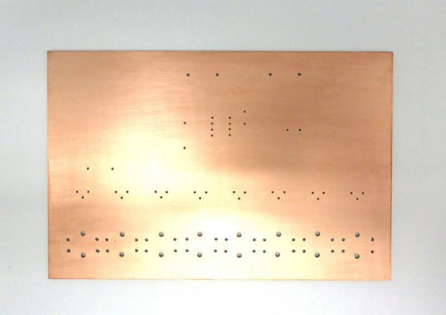
1. The stripped Board with holes.
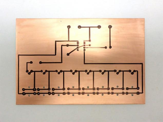
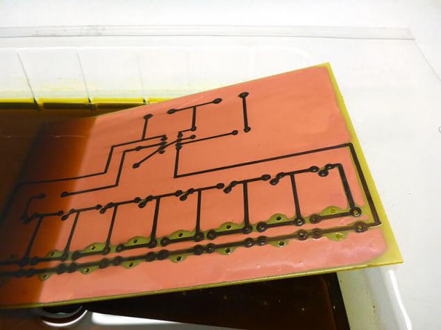
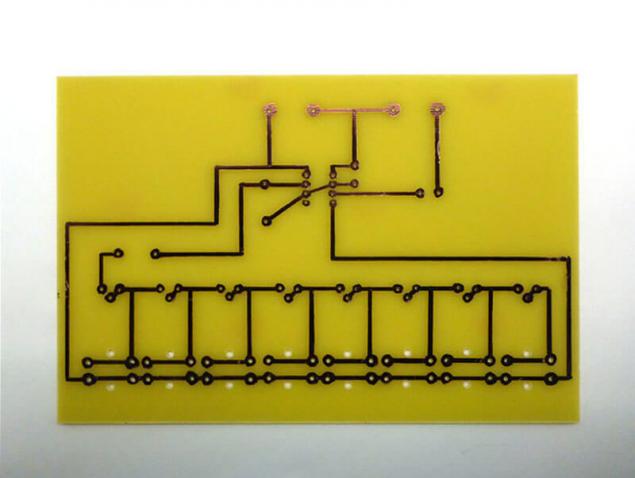
2. Board with printed marker pattern of conductors.
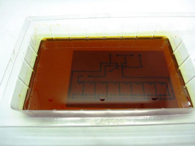
3. Cost of blister with ferric chloride solution immediately after immersion. The solution temperature is about 45 degrees.
4. The beginning of the process of etching the first protravlivayutsya the edge of a Board and the Board around the holes (about 5 min).
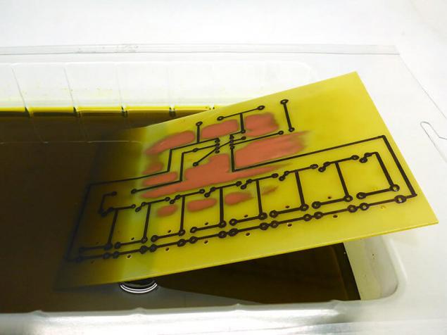
5. The continuation of the process after about 10 min. don't forget to waggle the blister to speed up the etching.
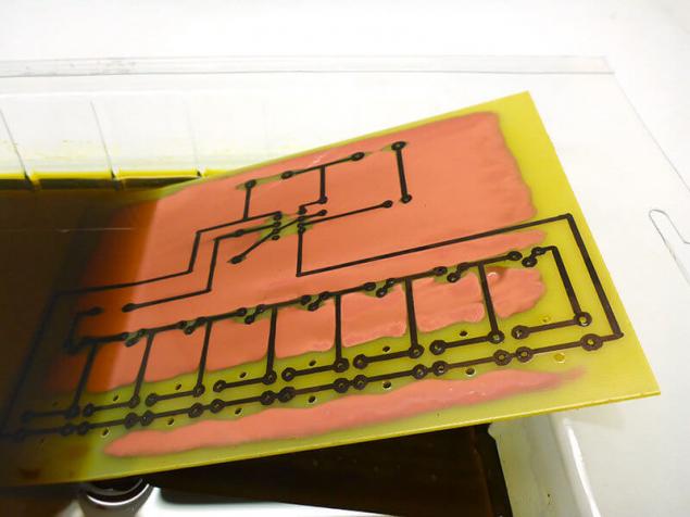
6. The etching is almost completed, and there small areas with a thin layer of foil. After about 15 min.
7. The etching is finished. After about 20 min.

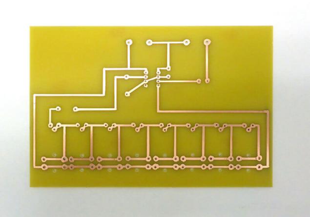
8. Board washed to remove traces of the marker
9. Traces of the pen removed, the conductors have not tinned.
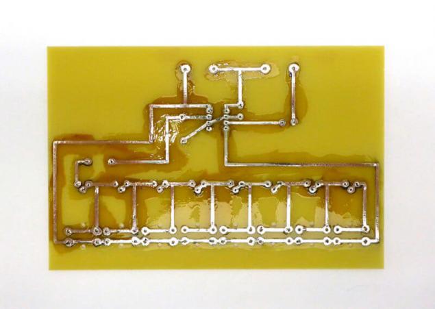
10. The flux conductors are deposited, after which they are tinned.
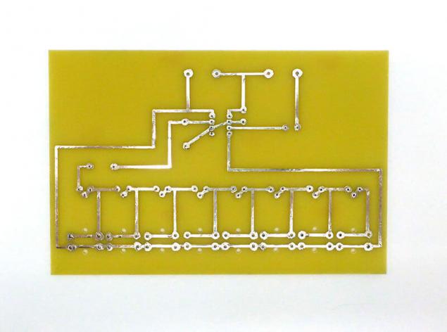
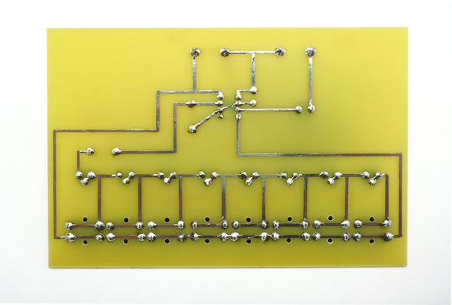
11. The conductors are tinned, flux laundered. Board ready for mounting and soldering components.
12. The view from the soldering after the components are installed.
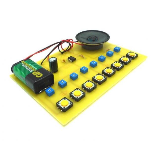
13. The device is assembled. published
P. S. And remember, only by changing their consumption — together we change the world! © Join us at Facebook , Vkontakte, Odnoklassniki
Source: geektimes.ru/company/masterkit/blog/264436/
Prologue
We are all consumers of electronic devices: phones, tablets, televisions, etc. But only one in a thousand has some understanding of how it all works "from the inside", and to create an electronic design from scratch with your own hands can really only be elected. We offer you to join the exclusive club. Read this material, and, if you're interested, try your hand at the exploration of man-made electronics!
Those of you who find the strength to read the article to the end, can proudly declare itself "I understand something in electronics manufacturing," and that he who commits a feat and overpower the Assembly of the proposed design, it is worthy the title of "real electronics-Profi" (well, almost).
This master class is based on a set of Master kit NN201, which includes the details and materials necessary for the manufacture of printed circuit boards and electronic piano. Of course, if you want all materials and tools can be purchased alone, only have to spend time searching and purchase of the necessary components.
The necessary theoretical minimum
Any electronic design contains dozens, or even hundreds or thousands of components: resistors, capacitors, diodes, chips, etc. All of these components have a certain way of electrically and mechanically interconnected.
The most simple circuits can be soldered "on a knee" - point wiring, but this construction turns out ugly, confusing, has a questionable mechanical rigidity. Therefore, in any serious electronic design must be something like a chassis on which are mounted all of the parts. In different years the chassis was made from metal, cardboard or plywood, but in the last 20-30 years technological standard chassis is a printed circuit Board.
A printed circuit Board is a sheet of dielectric material, the surface of which the specific configuration of the applied strip of conductive material (usually foil). As the basis is most often used glass fiber: it is incombustible and possesses high dielectric properties, and low cost. In fiberglass drilled holes in which pass the findings of the parts. On the reverse side of the Board insights are soldered to copper current-carrying conductors that are configured a certain way. Soldering is carried out thanks to the mechanical fixing of the components to the Board, and thanks to the copper conductive tracks of the conclusions of parts electrically connected to each other.
Of course, the copper track conductors in the appropriate places to stick the Board to the fiberglass. But technologically easier to do the opposite: take a sheet of the PCB is glued with a continuous layer of foil and remove the foil from unwanted places.
Remove the foil from the unnecessary areas is possible by mechanical means: by making a sharp knife cuts in necessary areas. However, this method is time-consuming, traumatic, and is suitable primarily for the most simple of the schemes.
The foil can be removed and the chemical method: it is sufficient to immerse the Board into the solution, corroding copper (usually is a ferric chloride solution). Only beforehand it is necessary to protect from exposure to solvent those portions of copper (future current-carrying conductors) that need to be saved. As such protective equipment is sometimes used varnish, but easier to draw paths with a special marker. Also in practice electronics, widespread so-called laser-crystal cabochons technology (LUT). In this method, the pattern of future current-carrying conductors printed on a laser printer on special paper. Then the paper is applied to the blank fiberglass and iron this "sandwich" and iron: as a result, toner particles remain on the workpiece and subsequently will not be pretreated with a solvent.
The process of removing the foil is called etching. Etching is continued depending on the concentration and temperature of the solution is from several minutes to hours. After the process fee was washed with water and removed the protective structure, which shall remain copper conductors.
Then is drilling holes for the components. Usually used microdrile and drill diameter of 0.8 to 1 mm. Copper oxidizes rapidly in the air, and this complicates soldering. Therefore, immediately before soldering, the cost should at least be cleaned with fine sandpaper, removing a layer of oxides. But it is best to cover copper conductors with a protective composition, a layer of solder. This process is called tinning and it helps to maintain the high degree of suitability of the Board for soldering for several years.
In a production environment on top of the conductive paths is applied to a so-called solder – mask-layer protective material. This layer protects the conducting paths from accidental short circuits and damage. Only the pads remain free from the mask that makes it easy to produce their ration.
Another fabrication process – silk-screen printing – it involves the application in the "front" side of the Board with a special paint symbols and inscriptions. It makes life easier for installers of the Board and its repair.
But in the home to carry out the processes of applying a solder mask and silkscreen is difficult, so we will not do this.
All PCBs are ready. After that, the cost of all the components are mounted and then soldered. Then, the resulting structure is configured and tested. In modern factories, most of these processes are industrial robots, but humans, so all going to do with their hands.
The long-awaited practice
Much more interesting to do not just boring printed circuit Board, and a fee on the basis of which it is possible to collect practically useful device. We will make a simple electronic musical instrument – a toy piano with 8 keys.
Materials and components that we need:
— processing of fiberglass foil with dimensions of no less than 10x15 cm;
— a marker (preferably varnish) or nail Polish to protect the conductive tracks (the token can be found in stationery shops and nail to borrow from mom/girlfriend/wife);
— ferric chloride – powder weighing 100 grams will be enough for the eye.
— drill and drill bits with a diameter of 0.8, 1.0 and 1.2 mm;
non — metallic tub (deep bowl) – it must fit our billet. Better to find some old unwanted capacity, because after our experiments, it probably will have to throw it away or continue to use for etching;
— rubber gloves to protect our hands from the solution.
Note that the kit Master kit includes the billet NN201 with the already drilled holes, special pen and a beautiful red jar of ferric chloride weighing 100g. The set comes in a plastic blister, which serves as a great tray for etching!
For soldering you need:
— soldering iron, pliers, solder, flux;
— radio, a list of which is given below.
All you need can be found in stores radios or household goods.
Schema-location pattern of current-carrying conductors of the printed circuit Board (looking from the side of the foil):

Preparing the PCB for etching
We clean the charge from the layer of copper fine-grained sandpaper (in the extreme case, suitable for rough ink eraser) and degrease with alcohol or gasoline;
Apply the template to the circuit Board and drill in the necessary holes;
Apply marker pattern of conductors and pads for the soldering of details, focusing on the wiring diagram and drilled holes, being careful not too much "slap" hands foil (so it is advisable to work in cotton gloves). In case of errors the marker is easily washed off with an alcohol solution. The dimensions of the contact pads under insights, you can do more (where space allows).
It is convenient to apply the drawings with a ruler, in two layers. After printing it is necessary to give the Board dry for about 10 minutes, then inspect the Board and correct any errors to finish, where the layer is thin, and procrasti with an awl or a thick needle seat incorrect merge tracks or pads.
Preparation of solutions and precautions
You must now prepare a solution of ferric chloride. For this purpose 100 grams of ferric chloride necessary to stir around 200-250 grams (one Cup) of warm water. Do not have to measure everything exactly to the gram: the process will go and at a slightly different ratio of ferric chloride and water, it is only necessary to note that the concentration of the solution and its temperature depends on the time of etching the Board.
In preparing the solution it is necessary to observe basic safety rules:
- to work in rubber gloves in a ventilated area!;
- not to lean close to the solution: stand out noxious fumes!;
- getting on the items, the solution leaves an indelible rusty spots, therefore, precautions should be taken that the powder or the solution does not get on surrounding objects!;
- to prepare the solution should be in glass or plastic container, but not metal, its solution will corrode!;
- stir the solution has to be plastic (very convenient disposable spoons) and wooden items (unnecessary pencil);
- the optimum solution temperature is 45-50 degrees;
Etching the Board
- Pour into a container of solution of ferric chloride;
- gently put the cost of the foil up into a solution so that a solution with a margin of 5-7 mm covers the entire cost;
- the duration of the process depends on the temperature and concentration of the solution and takes 10 to 30 minutes. It is desirable to reduce the time of etching jiggle blister, and the solution was stirred and was fresh in places of contact with the foil;
- visually observe the etching process: first, begin to bleed portions of the foil on the edges of the Board and near the drilled holes due to the fact that the solution in these places is in contact with the foil not only on the plane, but also on the cut foil;
- when all the excess foil will Strajitsa, carefully pour the solution into a container for later use or disposal.
- blister with foil placed under the jet of warm water and wash thoroughly (wear gloves!) blister and cost. Ensure that residues of active solution was diluted with water, before you get in the sink, yellow spots! You can start to place the blister in non-food container with water and start it washing;
- rinse the cost you need in the solution of any detergent or soap, it is possible to use a sponge dampened with water and detergent;
- cost finally wash with warm water, then dry it with a paper napkin;
- remove the protective layer marker, use alcohol applied to a sponge or cloth: wipe the charge several times until the protective layer is removed completely;
- again thoroughly wash the Board with detergent and dry (see above). If there is any doubt if the cost fat with your hands or any where else, it should again be cleaned and degreased costs. Then you don't have to touch the foil with your hands. The Board is almost ready!
- Covered conductors circuit Board layer spirtovodnogo flux (SCF) or neutral flux LTI-120;
- tinning is well-heated soldering iron with a flat tip;
- dip the tip of a soldering iron in rosin, and then take it a little bit of solder and apply the soldering iron tip to the track;
- keep sting for a few seconds so that the solder began to drip from the tip and spread on the heated conductor, and slowly advancing along the tip conductor to the solder to drag the tip and cover the track. Do not RUB the solder to the track: he spreads her myself, if the track is sufficiently warmed. The speed stinger is chosen empirically.
- Do not keep the soldering tip on one and the same portion of the Board more than a few seconds otherwise copper conductor can come unstuck from the Board;
- openings must remain free from solder. If the solder closed the hole, it is necessary to clean the soldering tip, dip it in resin and attach the stinger to this hole;
- similarly, it is necessary tinned with stinging all the tracks on the circuit Board.
Board is now ready for mounting and soldering components.
Description of the scheme
Consider the circuit of our design.
The scheme is built on the basis of the known chip NE555. IC chip included in a classic oscillator circuit whose frequency is determined by the capacitance C1 and the resistance between terminal "2" IC and "+" supply. When you press the buttons SW1...SW8 in customizados circuit chip includes a different potentiometer, respectively, BA1 speaker makes sounds of different pitch. As a result, even on such a basic musical instrument can play simple melodies.
Tool adjustment is made by trimming resistors VR1...VR8.
Circuit diagram:

Wiring diagram (side view detail):

We need the following details, which can be purchased at the hardware store; all these parts are included in the set NN201:
IC1 (IC chip) 1 PCs NE555P C1 (electrolytic capacitor) 10 UF 1 EA. C2 (ceramic capacitor) 0.1 µf 1 PC R1, R2 (resistors) 10K 0.25 W 2 PCs SW1-SW8 (button) B3F4005 8 pieces R3-R10 (resistor trimming) 3362P-1-103LF 8 PCs SP1 (speaker) 0.5 W 8R 1 PCs B1 (battery terminal) 1 PC. Mounting and soldering the Board
- mounted on the all components, focusing on the list, and wiring diagram;
- pay attention to correct orientation of the chip (the key in the form of a semi-circular recess in the top of the chip should be oriented as shown on the wiring diagram) and electrolytic capacitor (negative terminal marked on its body gray stripe and sign "-"; mounting scheme is specified output "+" of the capacitor);
- the parts do not fall out of the PCB, sinem their conclusions from the current-carrying tracks;
- cut the the components. Ideally, the conclusion should not be more than 2-3 mm from the axis of the hole.
- solder all the pins;
- check the quality of soldering: no neprodanih of conclusions and spurious closures, if necessary, eliminate errors.
Connected to the flow head and battery type "Crown". If the Board is made correctly, and the soldering made accurately, then when you press each of the buttons speaker should play the sound. Now it is necessary to adjust trimmer VR1-VR8 tones of each of the eight buttons, focusing on a real piano or a synth (you can install on your phone or tablet the appropriate program) or private hearing.
The setting should start with the resistor VR8. It corresponds to the highest tone. Press the SW8 button and rotate a thin screwdriver resistor VR8. The sound from the speaker must comply with any note of the second octave, for example. The next note should be a semitone below the si of the first octave. Press the SW7 button and rotate the resistor SW7, the next note is lower in tone, and so on with each button. After setting all eight notes get the full octave.
Now you can enjoy the result of the work and try to play a few simple tunes!
Application: photo gallery of the process of etching the Board
1. The stripped Board with holes.

2. Board with printed marker pattern of conductors.

3. Cost of blister with ferric chloride solution immediately after immersion. The solution temperature is about 45 degrees.

4. The beginning of the process of etching the first protravlivayutsya the edge of a Board and the Board around the holes (about 5 min).

5. The continuation of the process after about 10 min. don't forget to waggle the blister to speed up the etching.

6. The etching is almost completed, and there small areas with a thin layer of foil. After about 15 min.

7. The etching is finished. After about 20 min.

8. Board washed to remove traces of the marker

9. Traces of the pen removed, the conductors have not tinned.

10. The flux conductors are deposited, after which they are tinned.

11. The conductors are tinned, flux laundered. Board ready for mounting and soldering components.

12. The view from the soldering after the components are installed.

13. The device is assembled. published
P. S. And remember, only by changing their consumption — together we change the world! © Join us at Facebook , Vkontakte, Odnoklassniki

Source: geektimes.ru/company/masterkit/blog/264436/