401
Scientists have found a new material for flat semiconductors
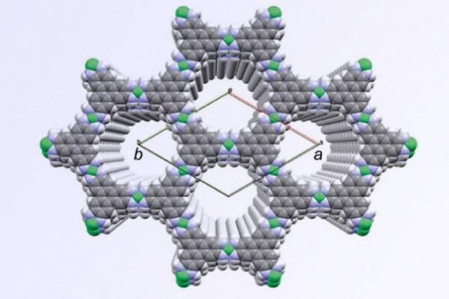
Scheme of the molecular structure of the new material shows how it forms a hexagonal lattice structure, and its two-dimensional layers.
Researchers have developed a two-dimensional, self-organizing material, which can produce solar panels or transistors.
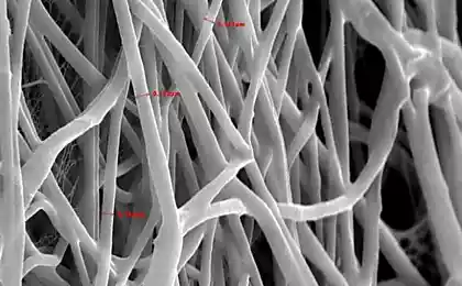
Engineers at mit and Harvard University have discovered two-dimensional material whose properties are very similar to graphene, but have some obvious advantages to a thin carbon layer. The new material is a combination of Nickel and an organic compound called HITP. By changing the proportions of ingredients, scientists can control and set the properties of the new material. The new compound Ni 3 (HITP) 2 has a hexagonal honeycomb structure. Several layers of material to form a perfectly smooth stack, with holes in the centers of the hexagons, measuring about 2 nanometers in diameter.
Associate Professor Mircea Dink said these cells have the ability to capture light waves of different lengths. And it can be used for supercapacitors that can store electrical energy unclaimed. Chemist, University of California Pingin Feng says: "This finding represents a major step forward in synthetic design of new semiconductor materials."
newsoffice.mit.edu/2014/new-material-flat-semiconductors-0430
Source: nauka24news.ru/