455
Opened new optoelectronic properties of perovskites
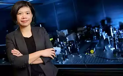
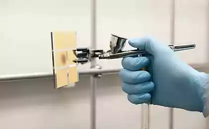
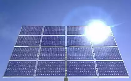
In search of solar cells and LEDs a new generation of American scientists from the National laboratory in Los Alamos has created an innovative two-dimensional hybrid perovskites, which will allow to make advanced optoelectronic devices: detectors, laser diodes, cheap solar panels.
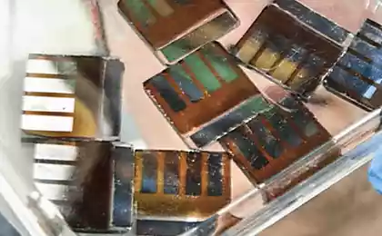
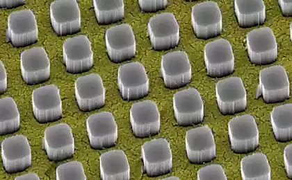
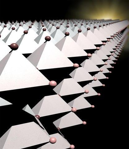
"Our material is a multi — layered structure consisting of stacks of two-dimensional perovskite layers with nanometer thickness (as a pack of sheets), where the perovskites are separated by thin organic layers," says Jean-Christophe Blancon, the lead author of an article published in the journal Science.
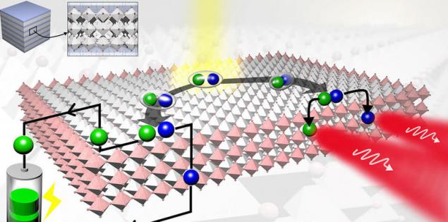
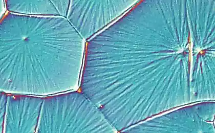
Two-dimensional perovskites Ruddlesden — Popper are quantum wells, in which the energy gap can be set by changing the thickness perovskite layer. Discovery scientists contradicts classical quantum systems in which electrons and holes are tightly bound by the Coulomb interaction of the excitons. Photophysical thin films of perovskites Ruddlesden — Popper with a thickness of 1.3 nm is controlled to the low-energy States associated with the electronic structure of the edges perovskite layers. These States open a direct path to the disintegration of excitons to free carriers, which greatly improve the performance of optoelectronic devices.
"It's a quantum hybrid materials with physical properties as organic semiconductors, and inorganic semiconducting quantum wells. We are only beginning to understand the relationship of organic and inorganic components in two-dimensional perovskites, and this result helps explain how the unique properties arise from the competition of the physical properties," says Jared Crochet, study participant.
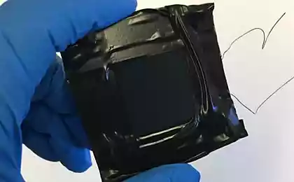
Two-dimensional hybrid perovskites continue to amaze scientists. "When we first created these materials, we hoped that high quality samples will have new optoelectronic properties, says study co-author mercury Kanatzidis from northwestern University. They exceeded our expectations and proved that he is a truly amazing system. We just lifted the edge of the curtain that is inside this two-dimensional family, and look forward to new discoveries".
The unique properties of perovskites used and the scholars of the Polytechnic school of Lausanne, who offered to create hard disks of new generation. Crystal structure of the new material combines the advantages of ferromagnetic materials and photoconductors. This combination creates a completely new phenomenon: a "melt" of magnetization under the influence of photoelectrons. published
P. S. And remember, only by changing their consumption — together we change the world! ©
Source: hightech.fm/2017/03/11/perovskite-device
"Our material is a multi — layered structure consisting of stacks of two-dimensional perovskite layers with nanometer thickness (as a pack of sheets), where the perovskites are separated by thin organic layers," says Jean-Christophe Blancon, the lead author of an article published in the journal Science.

Two-dimensional perovskites Ruddlesden — Popper are quantum wells, in which the energy gap can be set by changing the thickness perovskite layer. Discovery scientists contradicts classical quantum systems in which electrons and holes are tightly bound by the Coulomb interaction of the excitons. Photophysical thin films of perovskites Ruddlesden — Popper with a thickness of 1.3 nm is controlled to the low-energy States associated with the electronic structure of the edges perovskite layers. These States open a direct path to the disintegration of excitons to free carriers, which greatly improve the performance of optoelectronic devices.
"It's a quantum hybrid materials with physical properties as organic semiconductors, and inorganic semiconducting quantum wells. We are only beginning to understand the relationship of organic and inorganic components in two-dimensional perovskites, and this result helps explain how the unique properties arise from the competition of the physical properties," says Jared Crochet, study participant.

Two-dimensional hybrid perovskites continue to amaze scientists. "When we first created these materials, we hoped that high quality samples will have new optoelectronic properties, says study co-author mercury Kanatzidis from northwestern University. They exceeded our expectations and proved that he is a truly amazing system. We just lifted the edge of the curtain that is inside this two-dimensional family, and look forward to new discoveries".
The unique properties of perovskites used and the scholars of the Polytechnic school of Lausanne, who offered to create hard disks of new generation. Crystal structure of the new material combines the advantages of ferromagnetic materials and photoconductors. This combination creates a completely new phenomenon: a "melt" of magnetization under the influence of photoelectrons. published
P. S. And remember, only by changing their consumption — together we change the world! ©
Source: hightech.fm/2017/03/11/perovskite-device