799
3D microchip, is 1,000 times faster than existing
Scientists have invented a new method for the development and creation of computer microchips, which can significantly speed up processing at least 1000 times in comparison with the existing CPU. This technique is based on a material called carbon nanotubes, and allows for a microchip in three dimensions.
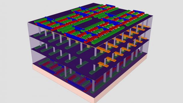
According to Max Shalakera (Max Shulaker), a member of the team of designers of the chip and the candidate for a doctorate in electrical engineering from Stanford University, California, a 3D design saves space in the system and increases the speed of data processing. This is achieved by the fact that scientists can hold a memory storing data and condense the number of processors into a miniature space.
Reducing the distance between the two elements can at times to speed up the processing time a computer commands.

Photos of Max Shalakera.
Slow progress h5> Computational capabilities of computer systems over the past 50 years constantly improved. This is largely due to the ability to continuously reduce the silicon transistors and a three-pronged switches is performing logical operations.
Communication problems h5> According Shalakera, one of the main obstacles in the processing speed of a computer memory.
Carbon nanotubes h5> To work around the problem with a temperature difference, the team at Stanford University turned its attention to open about 10 years ago, one-dimensional carbon material - carbon nanotubes. It - extended cylindrical mesh structure of the carbon atoms in diameter from one to several tens of nanometers. Processing capabilities at a low temperature have been key in selecting the material for an alternative to silicon. The processing temperature of just 200 a sup> C.

According to Max Shalakera (Max Shulaker), a member of the team of designers of the chip and the candidate for a doctorate in electrical engineering from Stanford University, California, a 3D design saves space in the system and increases the speed of data processing. This is achieved by the fact that scientists can hold a memory storing data and condense the number of processors into a miniature space.
Reducing the distance between the two elements can at times to speed up the processing time a computer commands.

Photos of Max Shalakera.
Slow progress h5> Computational capabilities of computer systems over the past 50 years constantly improved. This is largely due to the ability to continuously reduce the silicon transistors and a three-pronged switches is performing logical operations.
According to Moore's Law - a rough rule formulated by Gordon E. Moore (Gordon E. Moore) in 1965, the number of silicon transistors on a chip should double every two years. What is true for the further following a rule, you need to reduce tiny silicon transistors to 5 nanometers. But there is a problem - the limit for silicon, which is 7 nanometers (for comparison - the value of a human hair averages around 100,000 nanometers). The subsequent reduction of the scale will lead to the effect that the quantum particle can destroy their functioning. Accordingly, Moore's Law will come to its logical end in the next ten years. Furthermore, an infinite increase in the number of transistors on a chip - is not the only method of increasing the system performance.
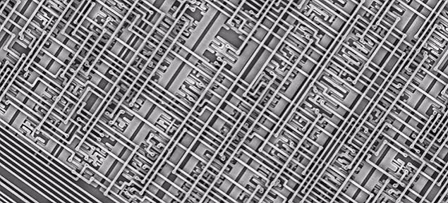
The transistors on modern-day circuits. (Photo by electron microscope.)

Communication problems h5> According Shalakera, one of the main obstacles in the processing speed of a computer memory.
Processing large amounts of data require query to a previously unknown data which have not yet been brought into the cache. In such cases it takes a long time to make a new request. The request for information for the processing of a team will go first to the internal cache of the processor. Then, after searching all levels of cache yielded responses that result is not the kernel sends a request to the RAM. After a search of memory, again, the answer will come, nothing found. And only then the request will be sent to the HDD or SSD drive. The signal will have to pass on the relatively thick (for electrons) wire, overcoming constant resistance. Agree, this is way too long and for the length of time the kernel has managed several times to complete the process.
If you perform this query instead of your PC, then 96% of the time was to wait. It is also worth remembering that even when the CPU is waiting for the desired manual, it still consumes energy. Alternatively, the offer may be combined CPU and memory on a single wafer. Just do not get to place these two components on the same plate - silicon wafer requires heating of 1000 a sup> C, causing melting of the metal elements of solid state drive or hard disk.
Carbon nanotubes h5> To work around the problem with a temperature difference, the team at Stanford University turned its attention to open about 10 years ago, one-dimensional carbon material - carbon nanotubes. It - extended cylindrical mesh structure of the carbon atoms in diameter from one to several tens of nanometers. Processing capabilities at a low temperature have been key in selecting the material for an alternative to silicon. The processing temperature of just 200 a sup> C.
CNT (carbon nanotubes) have the properties of electrical conductivity equal to silicon transistors, but their electrical properties depend on the angle of twist hexagonal graphite plane. Thus, the scientists were able to achieve higher conductivity by 5 orders of magnitude.
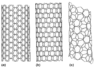
Three examples of nanotubes.
When compared to silicon transistors CNT under the same conditions and with the same architecture, the concept of device, the nanotubes are significantly faster performance, while consuming less power.
Nevertheless nanotubes grow randomly and more like a cup cooked spaghetti. Naturally this is not an option for the production of microchips. Researchers have developed a method of growing CNTs in narrow grooves, giving it a purposeful growth. But it did not solve all the problems. While the 99, 5% nanotubes grow ordered, 5% stubbornly refuse grow planned route. Out of this situation was a bit unexpected. The holes in the area of defective CNTs allow the chip to operate exactly as expected, neutralizing the growth defects of nanotubes.
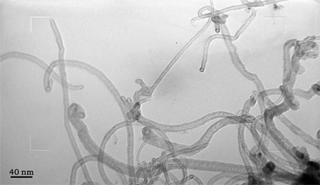
The growth of nanotubes. (Photo by electron microscope.)
Another problem arose prophesied to destroy the whole idea. Although most semiconductivity grown tubes is silicon, and the rest has a conductivity of conventional metal. Unfortunately, scientists have found it difficult to predict which tubes are defective. These few CNT could destroy the entire chip. But here, we found a solution - Shalaker and his colleagues simply filed for huge chip voltage pulses. Thus, the conductors were as fuse blown by the high voltage. And there were only chip semiconductors.
This team has already created a computer-based CNT, but it was slow and cumbersome with a relatively small number of transistors. The processor of the device is comparable in power to the Intel 4004, released in 1971. The first processor-based nanotubes comprises transistor 178 and their approximate length ranged from 10 to 200 nanometers.
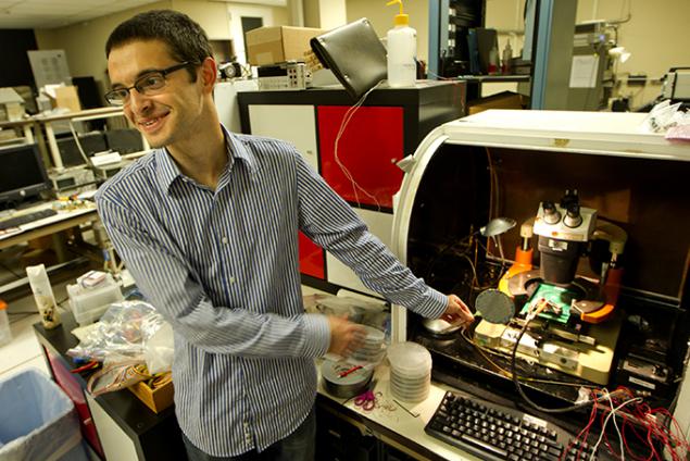
Max Shalaker in his hands earlier produced wafer with chips based on silicon nanotubes.
Now, researchers led by Shalakerom created a system for stacking memory along with the transistor layers, connecting them with tiny layers. The new structure saves time and requests, respectively, while fully processing the command. In 1000 times faster than similar systems of equal capacity. Using the new architecture, the team created a set of sensor plates that detect everything - from infrared light to certain chemicals in the environment.
Previously, I wrote an article about an alternative to silicon as semiconductor-based InGaAs . Here's another, in the form of carbon nanotubes.
And what alternative to silicon as the semiconductor, you know? Which of them are suitable for microchips of the future?
Source: geektimes.ru/company/ua-hosting/blog/263026/


Burnt by the Sun
Scientists announced the unambiguous evidence for the presence of liquid water on Mars