1721
Thermal barriers, tombstones and other delights of printed circuit boards
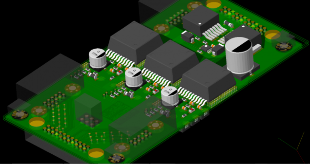
While steep designers design the right dress and bought ultramodern production at US-European plants, we turn to the experience of PCB design possibilities for urgent production of one of the suburban (actually Zelenograd - District of Moscow) plants with manual installation basement (actually at hand installers They sit right on the second floor and in the basement of the line stands at 60, 000 components per hour).
The following text - the personal opinion of the author. This is not the ultimate truth, but only one of the possible sections of the enormous amount of information that is available currently normal constructor. I>
Talk a little bit about CAD. Despite the fact that a lot of them, almost all of them make available to the designer about the same basic functionality. Possessing the necessary knowledge, can and Sprint-Layout (no offense!) To make high-speed dif.paru which will work fine. The only question is how long it takes the trace of the pair.
It is possible to nakosyachit in the same way PADS ("work with tracing" with Electronics replete with examples of interesting designs), which will have to disentangle long and tedious:
What is this? And the fact that if a designer - an idiot, no ultra-modern CAD will not solve the design problem for him. Yes, it will check all kinds of rules and a lot more. But consider absolutely everything possible. Especially in terms of soldering and assembly (although placement test recently getting better and better).
Unfortunately, the design of PP often found absolutely paragraphs are mutually exclusive. A typical example - bypass capacitors on the power supply. On the one hand it is necessary to place them as close to the power pin chips.
On the other hand, do not place components right next to each other, if you plan to automatic installation (you never know what the limitations of the particular machine, which will be set components) and reflow soldering (capacitor can be in the so-called "shadow" of the high component and heating the paste on his pads melted as it should).
And yet we must not forget about the frequencies at which we all work and inductance paths from \ to the capacitor affect its properties in a particular scheme (strongly recommend reading eto and here it for a better understanding of the issue).
But back to our stones and barriers. If you do not know what to do, what to do? Read the documentation, of course! And it is, and a lot!
Will not touch our guests, some of which have not been updated for more than forty years. To look at the standards of IPC, which have enjoyed great (ungrounded personal opinion of the author, because they do not know the exact numbers) of the PCB designers worldwide.
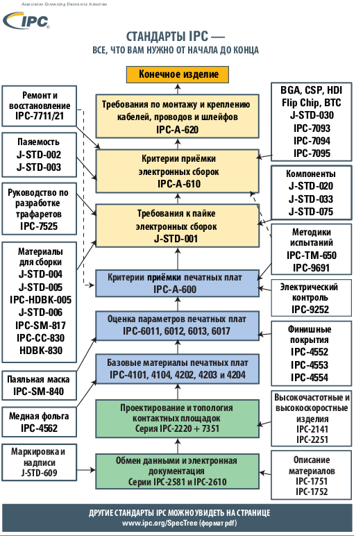
In the tree, standards can be seen that above all you can read something from 2220 and 7351.
From 2220, we are primarily interested in 2221 - Generic Standard on Printed Board Design . By reference the previous version of the standard, because the current only for the money (well, we know that everything is possible if you want to find).
In particular thermal barriers written about in Section 9.1.3. Briefly translate what is written there, it all comes down to the fact that if the component output (and 2221 is dedicated exclusively terminal components), the it is desirable i> to make thermal barriers, because their presence makes it easier to solder.
Now let's see what the thermal barrier:
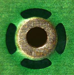
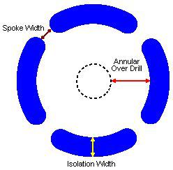
And what is it helps?
Well, firstly, with wave soldering.
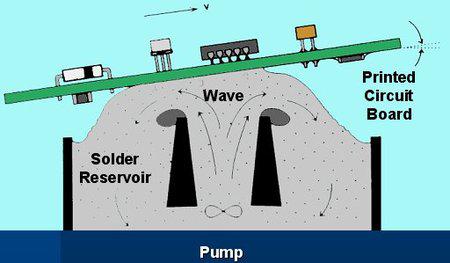
This type of solder is mainly used in very large-scale production. In this case, for a wave solder has a number of restrictions on the placement of components and a lot of advice on landing sites for the components.
Dave, as always, simply and clearly explains what's what:
Optimization, in a word, in order to reduce the number of marriages.
Interesting process:
The problem here is that not all machines have a preheating zone, and it does not always help if large polygons. It turns out that if the conduct charge slowly warmed to more polygons, chances of overheating small components. Thermal barriers help to solve this problem. But the devil is in the details, as always.
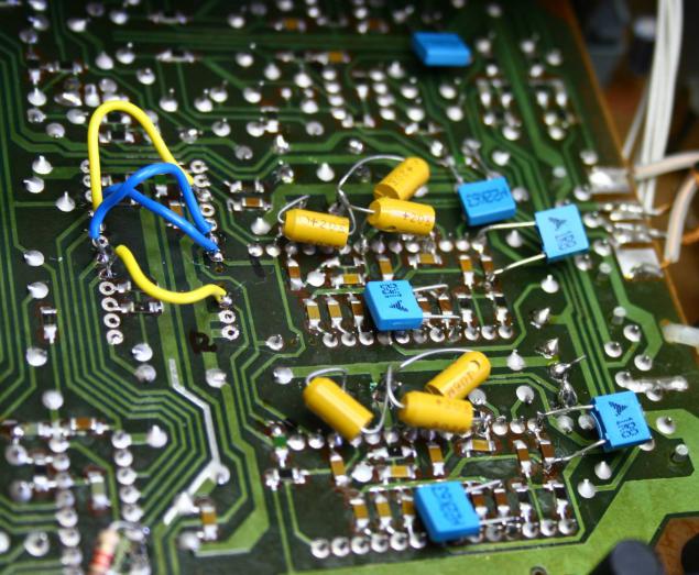
Before moving on, let's talk a little more about manual , not a machine soldering .
Imagine that you have a multilayer board as kdpv in the beginning, and it is necessary to solder connectors. But there is some problem in that six-layer board, with four layers of dull earth on the whole board. And half of connector - it land. You can, of course, take advantage of preheating to 100-110 degrees and then solder. But this is not always possible. Yes, and tantalum once again do not want to heat (after first was soldered all small things, and connectors in the least). Here thermal barriers and help. Soldering iron heats only the output connector, glass metallization and contact noses, not all polygons in all layers.
And this is where the problems begin.
It is clear that the thermal barrier reduces the total area of copper, through which the contact component and the landfill. That is, increasing physical contact resistance. Also increases parasitic inductance connections.
Pretty quick search showed that there are at least three articles in which we study the problem of resistance, inductance, and the relationship of all this.
Here they are:
A Demystifying Study of Thermal Relief Pads: Tradeoff between Manufacturing and Cooling li > Investigation on the Efficiency of Thermal Relief Shapes on Different Printed Circuit Boards a href="https://lirias.kuleuven.be/bitstream/123456789/400645/2/Thermal_reliefs_final.pdf"> Modeling the Low- and High-Frequency Impedance of Thermal Reliefs IEEE abbr>, which suggests that there is not frank delirium.
Again, I highly recommend to read.
The conclusions of all the articles in a nutshell: yes, thermal barriers - it's cool and useful, but you must use wisely (who would doubt it?). If in doubt, it is necessary at least prosimulirovat. Basically, it's the case of components for surface mounting, because of terminal components and so have sufficient stray inductance conclusions.
As for the resistance, then yes, it increases slightly at the contact point. About unity milliohms. If this is not critical, it is possible to use. And, of course, necessary to take into account the current which will flow through the connection. If he is, that is heating, you should see what is more important: some local overheating or ease of installation.
For myself, I brought this rule. On mock-ups can be safely used thermal barriers as models still mostly manually soldered. On serial products should consult with a particular production, which will be mounted board (it is not useful to do, in the sense to consult with the production), as the technology is better than you know your assembly line and its capabilities.
But it all came to terminal components. And how to be surface-mounted? But there is still more complicated. The standard 7351 - Generic Requirements for Surface Mount Design and Land Pattern Standard thermal barriers are not mentioned.
There are interesting document , in which the author advises not to use thermal barriers because of the increased impedance connection. Indeed, this makes sense: the design of power supplies and other power circuits.
Digress a bit.
I hope it looks like Placer components, many are.
If not, then here is a good illustration of the process:
After packing the board she goes on a conveyor oven reflow soldering.
It looks something like this:
Unfortunately, sometimes can have the following effect:
Its causes can be several (you can see the basic, for example, тут).
One of them - the curve термопрофиль soldering. Further there are (not in order of importance): overdue (or improperly stored) paste, stencil wrong to transfer paste crooked projected landing sites components Placer errors.
If thermoprofile, pasta, Placer and sometimes stencil - a headache production, the curves of the site - it is a direct jamb designer.
The main idea is that the site should be the same geometry that arose during the spreading paste the same surface tension forces. After lifting component arises because of the different surface tension forces that act on the planar component. It can also happen that the site is very large in itself (connection to the ground plane, for example), the thermal barrier is not present, and the crooked thermo pad warms more slowly than the other terminal. As a result, the paste will not melt at the polygonal area, and the component can rise.
A good illustration and сопутствующая Article :
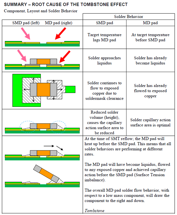
Why component rose? Because even if the cutout in the template was the same paste for both sites, then the process of melting the paste in order O, where most of the open area of the solder mask, not only heat is slower and the paste spread on a larger area, which is generally severely degrade the performance of the soldered connections (insufficient amount of solder) and may lead to a rotation component relative to the landing pad.
One outside Moscow, in the sense of Moscow, the office offers in this case a compromise:
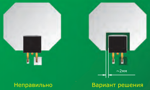
If there is a need in the large outdoor range of masks, to avoid spreading the paste on range, you can make a mask out of the locking bridge small width, which will prevent the spreading of the solder at melting.
All the above is mainly concerned with the light components with sizes less than 0603 (in inches), although there are exceptions.
What's the bottom line?
Thermal barriers, of course, necessary. Use them wherever you need and do not need to - not worth it. This is especially true of microwave technology. In everyday design simple microcontroller projects, in my opinion, they do more good than harm. But much depends on the soldering technology and the subsequent need for maintainability products.
When soldering in the furnace should be aware of the possibility of lifting components due to improper design of the landing sites and shoals technologist serving line.
In any case, Routing, primarily operate and analyze brain!
Thank you for reading!
All the bugs please report to the PM. The author continues to write about the development of the iron? Definitely yes Definitely not b my eyes have not seen you < / Voted 478 people. 70 people abstained. Only registered users can vote in polls. Sign , please.
Source: habrahabr.ru/post/246937/


